

 客服




最大带宽:20 MHz
模拟输出分辨率:14 bits
可支持的硬件平台:基于计算机的设备
总线连接:PCI
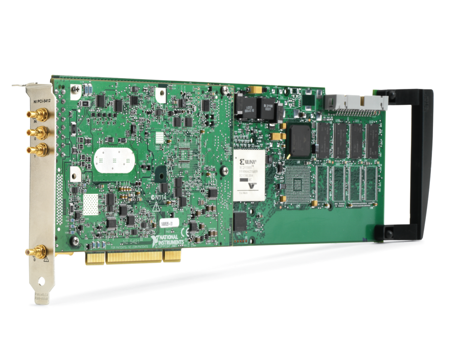
100 MS/s,14位波形发生器设备
ONETEST 欢迎您
厂商登录 | 入驻
登录 | 注册 购物车 微信公众号厂商登录
最大带宽:20 MHz
模拟输出分辨率:14 bits
可支持的硬件平台:基于计算机的设备
总线连接:PCI
100 MS/s,14位波形发生器设备
以下指标取自 Teledyne 官方在线规格书,按原文档小节分组。
| CLK IN | SMB |
| PFI 0 | Input/Output |
| CH 0 | Output |
| Number of channels | 1 |
| Connector type | SMB jack |
| Full-scale voltage Main output path[1] 12.00 V pk-pk to 5.64 mV pk-pk into a 50 Ω load | Main output path[1] |
| Main output path[1] | 12.00 V pk-pk to 5.64 mV pk-pk into a 50 Ω load |
| DAC resolution | 14 bits |
| Maximum output voltage[2] Low-gain amplifier path 50 Ω load ±1.000 Vpk 1 kΩ load ±1.905 Vpk Open load ±2.000 Vpk High-gain amplifier path 50 Ω load ±6.000 Vpk 1 kΩ load ±11.43 Vpk Open load ±12.00 Vpk | Low-gain amplifier path 50 Ω load ±1.000 Vpk 1 kΩ load ±1.905 Vpk Open load ±2.000 Vpk |
| Low-gain amplifier path 50 Ω load ±1.000 Vpk 1 kΩ load ±1.905 Vpk Open load ±2.000 Vpk | 50 Ω load |
| 50 Ω load | ±1.000 Vpk |
| 1 kΩ load | ±1.905 Vpk |
| Open load | ±2.000 Vpk |
| High-gain amplifier path 50 Ω load ±6.000 Vpk 1 kΩ load ±11.43 Vpk Open load ±12.00 Vpk | 50 Ω load |
| 50 Ω load | ±6.000 Vpk |
| 1 kΩ load | ±11.43 Vpk |
| Open load | ±12.00 Vpk |
| Amplitude range[], low-gain amplifier path 50 Ω load Minimum 0.00564 V pk-pk; maximum 2.00 V pk-pk 1 kΩ load Minimum 0.0107 V pk-pk; maximum 3.81 V pk-pk Open load Minimum 0.0113 V pk-pk; maximum 4.00 V pk-pk | 50 Ω load |
| 50 Ω load | Minimum 0.00564 V pk-pk; maximum 2.00 V pk-pk |
| 1 kΩ load | Minimum 0.0107 V pk-pk; maximum 3.81 V pk-pk |
| Open load | Minimum 0.0113 V pk-pk; maximum 4.00 V pk-pk |
| Amplitude range[], high-gain amplifier path 50 Ω load Minimum 0.0338 V pk-pk; maximum 12.0 V pk-pk 1 kΩ load Minimum 0.0644 V pk-pk; maximum 22.9 V pk-pk Open load Minimum 0.0676 V pk-pk; maximum 24.0 V pk-pk | 50 Ω load |
| 50 Ω load | Minimum 0.0338 V pk-pk; maximum 12.0 V pk-pk |
| 1 kΩ load | Minimum 0.0644 V pk-pk; maximum 22.9 V pk-pk |
| Open load | Minimum 0.0676 V pk-pk; maximum 24.0 V pk-pk |
| DC accuracy (calibrated for high-impedance load)[4] Within ±10 °C of self-calibration temperature ±0.2% of amplitude range ±0.05% of offset ±500 µV 0 °C to 55 °C ±0.4% of amplitude range ±0.05% of offset ±1 mV | Within ±10 °C of self-calibration temperature |
| Within ±10 °C of self-calibration temperature | ±0.2% of amplitude range ±0.05% of offset ±500 µV |
| 0 °C to 55 °C | ±0.4% of amplitude range ±0.05% of offset ±1 mV |
| AC amplitude accuracy[5] | (+2.0% + 1 mV), (-1.0% - 1 mV) (+0.8% + 0.5 mV), (-0.2% - 0.5 mV), typical |
| Output impedance | Software-selectable: 50 Ω or 75 Ω, nominal |
| Output coupling | DC |
| Output enable | Software-selectable[6] |
| Maximum output overload | CH 0 can be connected to a 50 Ω, ±12 V (±8 V for the direct path) source without sustaining any damage.[7] |
| Waveform summing | Supported[8] |
| Bandwidth[9] | 20 MHz |
| Digital interpolation filter[10] | Software-selectable: Finite impulse response (FIR) filter. Available interpolation factors are 2, 4, or 8. |
| Passband flatness[11] | ±1.0 dB from DC to 6 MHz |
| Pulse response[12] Low-gain amplifier path Rise/fall time <20 ns, typical Aberration <5%, typical High-gain amplifier path Rise/fall time <20 ns, typical Aberration <5%, typical | Low-gain amplifier path Rise/fall time <20 ns, typical Aberration <5%, typical |
| Low-gain amplifier path Rise/fall time <20 ns, typical Aberration <5%, typical | Rise/fall time |
| Rise/fall time | <20 ns, typical |
| Aberration | <5%, typical |
| High-gain amplifier path Rise/fall time <20 ns, typical Aberration <5%, typical | Rise/fall time |
| Rise/fall time | <20 ns, typical |
| Aberration | <5%, typical |
| Suggested maximum frequencies[13] Low-gain amplifier path Sine 20 MHz Square 5 MHz Ramp 1 MHz Triangle 1 MHz High-gain amplifier path Sine 20 MHz Square 5 MHz Ramp 1 MHz Triangle 1 MHz | Low-gain amplifier path Sine 20 MHz Square 5 MHz Ramp 1 MHz Triangle 1 MHz |
| Low-gain amplifier path Sine 20 MHz Square 5 MHz Ramp 1 MHz Triangle 1 MHz | Sine |
| Sine | 20 MHz |
| Square | 5 MHz |
| Ramp | 1 MHz |
| Triangle | 1 MHz |
| High-gain amplifier path Sine 20 MHz Square 5 MHz Ramp 1 MHz Triangle 1 MHz | Sine |
| Sine | 20 MHz |
| Square | 5 MHz |
| Ramp | 1 MHz |
| Triangle | 1 MHz |
| Spurious-free dynamic range (SFDR)[14] without harmonics[15] Low-gain amplifier path 1 MHz 70 dB, typical 10 MHz 65 dB, typical 20 MHz 60 dB, typical High-gain amplifier path 1 MHz 70 dB, typical 10 MHz 65 dB, typical 20 MHz 60 dB, typical | Low-gain amplifier path 1 MHz 70 dB, typical 10 MHz 65 dB, typical 20 MHz 60 dB, typical |
| Low-gain amplifier path 1 MHz 70 dB, typical 10 MHz 65 dB, typical 20 MHz 60 dB, typical | 1 MHz |
| 1 MHz | 70 dB, typical |
| 10 MHz | 65 dB, typical |
| 20 MHz | 60 dB, typical |
| High-gain amplifier path 1 MHz 70 dB, typical 10 MHz 65 dB, typical 20 MHz 60 dB, typical | 1 MHz |
| 1 MHz | 70 dB, typical |
| 10 MHz | 65 dB, typical |
| 20 MHz | 60 dB, typical |
| Total harmonic distortion (THD)[16] (0 °C to 40 °C) Low-gain amplifier path 1 MHz -59 dBc, typical 10 MHz -52 dBc, typical 20 MHz -45 dBc, typical High-gain amplifier path 1 MHz -51 dBc, typical 10 MHz -40 dBc, typical 20 MHz -37 dBc, typical | Low-gain amplifier path 1 MHz -59 dBc, typical 10 MHz -52 dBc, typical 20 MHz -45 dBc, typical |
| Low-gain amplifier path 1 MHz -59 dBc, typical 10 MHz -52 dBc, typical 20 MHz -45 dBc, typical | 1 MHz |
| 1 MHz | -59 dBc, typical |
| 10 MHz | -52 dBc, typical |
| 20 MHz | -45 dBc, typical |
| High-gain amplifier path 1 MHz -51 dBc, typical 10 MHz -40 dBc, typical 20 MHz -37 dBc, typical | 1 MHz |
| 1 MHz | -51 dBc, typical |
| 10 MHz | -40 dBc, typical |
| 20 MHz | -37 dBc, typical |
| Average noise density[17] Low-gain amplifier path 2 Vpk-pk, 10 dBm amplitude range 45 nV √Hz , -134 dBm/Hz, -144 dBFS/Hz, typical High-gain amplifier path 12 Vpk-pk, 25.6 dBm amplitude range 251 nV √Hz , -119 dBm/Hz, -145 dBFS/Hz, typical | Low-gain amplifier path 2 Vpk-pk, 10 dBm amplitude range 45 nV √Hz , -134 dBm/Hz, -144 dBFS/Hz, typical |
| Low-gain amplifier path 2 Vpk-pk, 10 dBm amplitude range 45 nV √Hz , -134 dBm/Hz, -144 dBFS/Hz, typical | 2 Vpk-pk, 10 dBm amplitude range |
| 2 Vpk-pk, 10 dBm amplitude range | 45 nV √Hz , -134 dBm/Hz, -144 dBFS/Hz, typical |
| High-gain amplifier path 12 Vpk-pk, 25.6 dBm amplitude range 251 nV √Hz , -119 dBm/Hz, -145 dBFS/Hz, typical | 12 Vpk-pk, 25.6 dBm amplitude range |
| 12 Vpk-pk, 25.6 dBm amplitude range | 251 nV √Hz , -119 dBm/Hz, -145 dBFS/Hz, typical |
| Sample rate range Divide-by-N 23.84 S/s to 100 MS/s High-Resolution 10 S/s to 100 MS/s CLK IN 200 kS/s to 105 MS/s RTSI<0..7> 10 S/s to 20 MS/s | Divide-by-N |
| Divide-by-N | 23.84 S/s to 100 MS/s |
| High-Resolution | 10 S/s to 100 MS/s |
| CLK IN | 200 kS/s to 105 MS/s |
| RTSI<0..7> | 10 S/s to 20 MS/s |
| Sample rate resolution Divide-by-N Configurable to (100 MS/s)/N(1 ≤ N ≤ 4,194,304) High-Resolution 1.06 µHz CLK IN and RTSI<0..7> Resolution determined by External Clock source. External Sample Clock duty cycle tolerance 40% to 60%. | Divide-by-N |
| Divide-by-N | Configurable to (100 MS/s)/N(1 ≤ N ≤ 4,194,304) |
| High-Resolution | 1.06 µHz |
| CLK IN and RTSI<0..7> | Resolution determined by External Clock source. External Sample Clock duty cycle tolerance 40% to 60%. |
| 1 (Off) | 10 S/s to 105 MS/s |
| 2 | 12.5 MS/s to 105 MS/s |
| 4 | 10 MS/s to 100 MS/s |
| 8 | 10 MS/s to 50 MS/s |
| Delay adjustment range Divide-by-N ±1 Sample Clock period High-Resolution ±1 Sample Clock period | Divide-by-N |
| Divide-by-N | ±1 Sample Clock period |
| High-Resolution | ±1 Sample Clock period |
| Delay adjustment resolution Divide-by-N <10 ps High-Resolution Sample Clock period/16,384 | Divide-by-N |
| Divide-by-N | <10 ps |
| High-Resolution | Sample Clock period/16,384 |
| System phase noise density offset[18] 100 Hz -90 dBc/Hz, typical 1 kHz -110 dBc/Hz, typical 10 kHz -120 dBc/Hz, typical | 100 Hz |
| 100 Hz | -90 dBc/Hz, typical |
| 1 kHz | -110 dBc/Hz, typical |
| 10 kHz | -120 dBc/Hz, typical |
| System output jitter (integrated from 100 Hz to 100 kHz)[18] | <7 ps rms, typical |
| External Sample Clock input jitter tolerance Cycle-cycle jitter ±300 ps, typical Period jitter ±1 ns, typical | Cycle-cycle jitter |
| Cycle-cycle jitter | ±300 ps, typical |
| Period jitter | ±1 ns, typical |
| Destinations[19] | PFI <0..1> (SMB front panel connectors) RTSI<0..6> |
| Maximum frequency PFI <0..1> 105 MHz RTSI<0..6> 20 MHz | PFI <0..1> |
| PFI <0..1> | 105 MHz |
| RTSI<0..6> | 20 MHz |
| Duty cycle PFI <0..1> 25% to 65% | PFI <0..1> |
| PFI <0..1> | 25% to 65% |
| Source | Internal Sample Clocks can either be locked to a Reference Clock using a phase-locked loop or derived from the onboard VCXO frequency reference. |
| Frequency accuracy | ±25 ppm |
| Sources[20] | PXI_CLK10 (backplane connector) CLK IN (SMB front panel connector) |
| Frequency accuracy | When using the PLL, the frequency accuracy of the PCI-5412 is solely dependent on the frequency accuracy of the PLL Reference Clock source. |
| Lock time | 200 ms, maximum 70 ms, typical |
| Frequency range[21] | 5 MHz to 20 MHz in increments of 1 MHz[22] |
| Duty cycle range | 40% to 60% |
| Destinations | PFI <0..1> (SMB front panel connectors) PXI_Trig <0..6> (backplane connector) |
| Connector type | SMB jack |
| Direction | Input |
| Destinations | Sample Clock PLL Reference Clock |
| Frequency range Sample Clock destination and sine waves 1 MHz to 105 MHz Sample Clock destination and square waves 200 kHz to 105 MHz PLL Reference Clock destination 5 MHz to 20 MHz | Sample Clock destination and sine waves |
| Sample Clock destination and sine waves | 1 MHz to 105 MHz |
| Sample Clock destination and square waves | 200 kHz to 105 MHz |
| PLL Reference Clock destination | 5 MHz to 20 MHz |
| Input voltage range into 50 Ω Sine wave 0.65 V pk-pk to 2.8 V pk-pk (0 dBm to +13 dBm) Square wave 0.2 V pk-pk to 2.8 V pk-pk | Sine wave |
| Sine wave | 0.65 V pk-pk to 2.8 V pk-pk (0 dBm to +13 dBm) |
| Square wave | 0.2 V pk-pk to 2.8 V pk-pk |
| Maximum input overload | ±10 V |
| Input impedance | 50 Ω |
| Input coupling | AC |
| Connector type | SMB jack (x2) |
| Direction | Bidirectional |
| Frequency range | DC to 105 MHz |
| As an input (trigger) Destinations Start Trigger Maximum input overload -2 V to +7 V V IH 2.0 V V IL 0.8 V Input impedance 1 kΩ | Destinations |
| Destinations | Start Trigger |
| Maximum input overload | -2 V to +7 V |
| V IH | 2.0 V |
| V IL | 0.8 V |
| Input impedance | 1 kΩ |
| As an output (event) Sources Sample Clock divided by integer K (1 ≤ K ≤ 4,194,304) Sample Clock Timebase (100 MHz) divided by integer M (2 ≤ M ≤ 4,194,304) PLL Reference Clock Marker Exported Start Trigger (Out Start Trigger) Output impedance 50 Ω Maximum output overload -2 V to +7 V Minimum V OH[23] Open load 2.9 V 50 Ω load 1.4 V Maximum V OL[23] Open load 0.2 V 50 Ω load 0.2 V Rise/fall time (20% to 80%)[24] ≤2.0 ns | Sources |
| Sources | Sample Clock divided by integer K (1 ≤ K ≤ 4,194,304) Sample Clock Timebase (100 MHz) divided by integer M (2 ≤ M ≤ 4,194,304) PLL Reference Clock Marker Exported Start Trigger (Out Start Trigger) |
| Output impedance | 50 Ω |
| Maximum output overload | -2 V to +7 V |
| Minimum V OH[23] Open load 2.9 V 50 Ω load 1.4 V | Open load |
| Open load | 2.9 V |
| 50 Ω load | 1.4 V |
| Maximum V OL[23] Open load 0.2 V 50 Ω load 0.2 V | Open load |
| Open load | 0.2 V |
| 50 Ω load | 0.2 V |
| Rise/fall time (20% to 80%)[24] | ≤2.0 ns |
| Sources | PFI<0..1> (SMB front panel connectors) RTSI<0..7> Software (use node or function call) Immediate (does not wait for a trigger). The default is Immediate. |
| Modes | Single Continuous Stepped Burst |
| Edge detection | Rising |
| Minimum pulse width | 25 ns |
| Delay from Start Trigger to CH 0 analog output Digital interpolation filter disabled 43 Sample Clock periods + 110 ns, typical Interpolation factor of 2 57 Sample Clock periods + 110 ns, typical Interpolation factor of 4 63 Sample Clock periods + 110 ns, typical Interpolation factor of 8 64 Sample Clock periods + 110 ns, typical | Digital interpolation filter disabled |
| Digital interpolation filter disabled | 43 Sample Clock periods + 110 ns, typical |
| Interpolation factor of 2 | 57 Sample Clock periods + 110 ns, typical |
| Interpolation factor of 4 | 63 Sample Clock periods + 110 ns, typical |
| Interpolation factor of 8 | 64 Sample Clock periods + 110 ns, typical |
| Destinations | A signal used as a trigger can be routed out to any destination listed in the Destinations specification of the Markers section |
| Exported trigger delay | 65 ns, typical |
| Exported trigger pulse width | >150 ns |
| Destinations | PFI <0..1> (SMB front panel connectors) RTSI<0..6> |
| Quantity | One marker per segment |
| Quantum | Marker position must be placed at an integer multiple of four samples. |
| Width | >150 ns |
| Skew RTSI<0..6> With respect to analog output ±2 Sample Clock periods | RTSI<0..6> With respect to analog output ±2 Sample Clock periods |
| RTSI<0..6> With respect to analog output ±2 Sample Clock periods | With respect to analog output |
| With respect to analog output | ±2 Sample Clock periods |
| Onboard memory size 8 MB standard 8,388,608 bytes 32 MB option 33,554,432 bytes 256 MB option 268,435,456 bytes | 8 MB standard |
| 8 MB standard | 8,388,608 bytes |
| 32 MB option | 33,554,432 bytes |
| 256 MB option | 268,435,456 bytes |
| Output modes | Arbitrary waveform[25] Arbitrary sequence[26] |
| Minimum waveform size Arbitrary waveform mode Single Trigger mode 16 samples Continuous Trigger mode 16 samples Stepped Trigger mode 32 samples Burst Trigger mode 16 samples Arbitrary sequence mode Single Trigger mode 16 samples Continuous Trigger mode 96 samples at >50 MS/s 32 samples at ≤50 MS/s Stepped Trigger mode 96 samples at >50 MS/s 32 samples at ≤50 MS/s Burst Trigger mode 512 samples at >50 MS/s 256 samples at ≤50 MS/s | Arbitrary waveform mode Single Trigger mode 16 samples Continuous Trigger mode 16 samples Stepped Trigger mode 32 samples Burst Trigger mode 16 samples |
| Arbitrary waveform mode Single Trigger mode 16 samples Continuous Trigger mode 16 samples Stepped Trigger mode 32 samples Burst Trigger mode 16 samples | Single Trigger mode |
| Single Trigger mode | 16 samples |
| Continuous Trigger mode | 16 samples |
| Stepped Trigger mode | 32 samples |
| Burst Trigger mode | 16 samples |
| Arbitrary sequence mode Single Trigger mode 16 samples Continuous Trigger mode 96 samples at >50 MS/s 32 samples at ≤50 MS/s Stepped Trigger mode 96 samples at >50 MS/s 32 samples at ≤50 MS/s Burst Trigger mode 512 samples at >50 MS/s 256 samples at ≤50 MS/s | Single Trigger mode |
| Single Trigger mode | 16 samples |
| Continuous Trigger mode | 96 samples at >50 MS/s 32 samples at ≤50 MS/s |
| Stepped Trigger mode | 96 samples at >50 MS/s 32 samples at ≤50 MS/s |
| Burst Trigger mode | 512 samples at >50 MS/s 256 samples at ≤50 MS/s |
| Loop count | 1 to 16,777,215 Burst trigger: Unlimited |
| Quantum | Waveform size must be an integer multiple of four samples. |
| Maximum waveform memory, arbitrary waveform mode 8 MB standard 4,194,176 samples 32 MB option 16,777,088 samples 256 MB option 134,217,600 samples | 8 MB standard |
| 8 MB standard | 4,194,176 samples |
| 32 MB option | 16,777,088 samples |
| 256 MB option | 134,217,600 samples |
| Maximum waveform memory, arbitrary sequence mode[28] 8 MB standard 4,194,120 samples 32 MB option 16,777,008 samples 256 MB option 134,217,520 samples | 8 MB standard |
| 8 MB standard | 4,194,120 samples |
| 32 MB option | 16,777,008 samples |
| 256 MB option | 134,217,520 samples |
| Maximum waveforms, arbitrary sequence mode[28] 8 MB standard 65,000 Burst trigger: 8,000 32 MB option 262,000 Burst trigger: 32,000 256 MB option 2,097,000 Burst trigger: 262,000 | 8 MB standard |
| 8 MB standard | 65,000 Burst trigger: 8,000 |
| 32 MB option | 262,000 Burst trigger: 32,000 |
官方规格书:https://www.ni.com/docs/en-US/bundle/pci-5412-specs/page/specs.html
NI官方渠道
官方渠道(官网 / 热线 / 邮箱)
官方渠道(中国大陆)
• 官网 www.ni.com/zh-cn
• 在线选购 www.ni.com/zh-cn/shop.html
• 经销商查询
官网「查找经销商」 www.ni.com/zh-cn/shop/advisors.html
• 联系方式
NI 中文官网不公布中国区电话与邮箱,报价、技术支持、校准、维修一律通过官网在线表单提交(「联系我们」页)
全国办事处
公司总部
• NI(National Instruments)
• 地址
11500 N Mopac Expwy, Austin, TX 78759-3504, United States
• 母公司
Emerson(2023 年完成收购,NI 隶属艾默生测试与测量业务集团)
0条提问
X
提问
X
回答
发表口碑

AI问答



 粤公网安备44030902003758