

 客服




最大带宽:40 MHz
输出通道数量:1
模拟输出电压范围:-5 V 至 5 V
模拟输出板载内存大小:32 kB
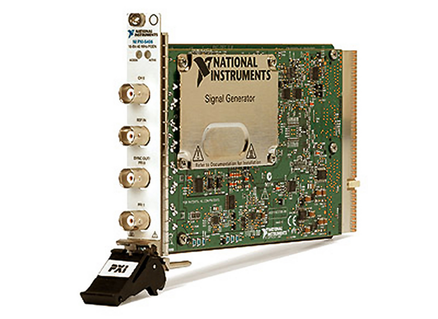
40 MHz带宽,1通道,16位PXI波形发生器
ONETEST 欢迎您
厂商登录 | 入驻
登录 | 注册 购物车 微信公众号厂商登录
最大带宽:40 MHz
输出通道数量:1
模拟输出电压范围:-5 V 至 5 V
模拟输出板载内存大小:32 kB
40 MHz带宽,1通道,16位PXI波形发生器
以下指标取自 Teledyne 官方在线规格书,按原文档小节分组。
| CH 0 | BNC |
| REF IN | Input |
| SYNC OUT/PFI 0 | Input/Output |
| PFI 1 | Accepts a trigger from an external source and can start or step through waveform generation or route signals from several clock, event, and trigger sources. |
| No color (off) | The PXI-5406 is not yet functional, or the PXI-5406 has detected a problem with a power rail. |
| Amber | The PXI-5406 is being accessed. |
| Green | The PXI-5406 is ready to be programmed by NI-FGEN. |
| No color (off) | The PXI-5406 is not generating. |
| Amber | The PXI-5406 is armed and waiting for a trigger. |
| Green | The PXI-5406 has received a trigger and is generating a waveform. |
| Number of channels | 1 |
| Connector type | BNC |
| Maximum voltage | ±5 V (ACpk + DC) |
| DAC resolution | 16 bits |
| Amplitude range[2] 50 Ω load 5.64 mVpk-pk to 10 Vpk-pk High-impedance load 11.28 mVpk-pk to 20 Vpk-pk | 50 Ω load |
| 50 Ω load | 5.64 mVpk-pk to 10 Vpk-pk |
| High-impedance load | 11.28 mVpk-pk to 20 Vpk-pk |
| Amplitude resolution | <0.06% (0.004 dB) of amplitude range |
| Offset range[3] Square waveforms ±50% of amplitude range All other waveforms ±5 V | Square waveforms |
| Square waveforms | ±50% of amplitude range |
| All other waveforms | ±5 V |
| AC amplitude accuracy[4] | +2.0% of amplitude +1 mV -1.0% of amplitude -1 mV |
| Offset accuracy[5] | ±0.5% of offset ±2 mV±0.5% of amplitude |
| Output impedance | Software-selectable: 50 Ω or 75 Ω |
| Output enable | Software-selectable: When the output path is disabled, the CH 0 output is terminated to ground with a 1 W resistor with a value equal to the selected output impedance |
| Maximum output overload | The CH 0 output can be connected to a 50 Ω, ±12 V source without sustaining any damage. No damage occurs if the CH 0 output is shorted to ground indefinitely. |
| Waveform summing | Outputs of multiple PXI-5406 signal generators can be connected together |
| Phase adjustment | -180° to +180° |
| Digital interpolation filter[6] | Software-selectable: Finite Impulse Response (FIR) filter with available interpolation factors of 2 or 4 |
| Analog filter | Software-selectable: 7-pole elliptical filter |
| Frequency resolution | 0.355 μHz |
| Maximum frequencies[7] Sine 40 MHz Square 25 MHz Ramp 5 MHz Triangle 5 MHz User-defined[8] 40 MHz | Sine |
| Sine | 40 MHz |
| Square | 25 MHz |
| Ramp | 5 MHz |
| Triangle | 5 MHz |
| User-defined[8] | 40 MHz |
| Maximum sample rate Sine 400 MS/s Square 400 MS/s Ramp 100 MS/s Triangle 100 MS/s User-defined[8] 400 MS/s Noise 100 MS/s | Sine |
| Sine | 400 MS/s |
| Square | 400 MS/s |
| Ramp | 100 MS/s |
| Triangle | 100 MS/s |
| User-defined[8] | 400 MS/s |
| Noise | 100 MS/s |
| Passband flatness[9] | ±0.4 dB (±5%) |
| Spurious-free dynamic range (SFDR)[10] with harmonics[11] <10 MHz 50 dB, typical 10 MHz to 40 MHz 45 dB, typical | <10 MHz |
| <10 MHz | 50 dB, typical |
| 10 MHz to 40 MHz | 45 dB, typical |
| Spurious-free dynamic range (SFDR)[10] without harmonics[12] <20 MHz 70 dB, typical 20 MHz to 40 MHz 60 dB, typical | <20 MHz |
| <20 MHz | 70 dB, typical |
| 20 MHz to 40 MHz | 60 dB, typical |
| Total harmonic distortion (THD)[13] DC to 1 MHz ≤1.66 Vpk-pk –60 dBc, typical >1.66 Vpk-pk –58 dBc, typical 1 MHz to 40 MHz ≤1.66 Vpk-pk –41 dBc >1.66 Vpk-pk –32 dBc | DC to 1 MHz ≤1.66 Vpk-pk –60 dBc, typical >1.66 Vpk-pk –58 dBc, typical |
| DC to 1 MHz ≤1.66 Vpk-pk –60 dBc, typical >1.66 Vpk-pk –58 dBc, typical | ≤1.66 Vpk-pk |
| ≤1.66 Vpk-pk | –60 dBc, typical |
| >1.66 Vpk-pk | –58 dBc, typical |
| 1 MHz to 40 MHz ≤1.66 Vpk-pk –41 dBc >1.66 Vpk-pk –32 dBc | ≤1.66 Vpk-pk |
| ≤1.66 Vpk-pk | –41 dBc |
| >1.66 Vpk-pk | –32 dBc |
| Signal to Noise and Distortion (SINAD)[12] DC to 1 MHz ≤1.66 Vpk-pk 58 dBc >1.66 Vpk-pk 58 dBc 1 MHz to 40 MHz ≤1.66 Vpk-pk 41 dBc >1.66 Vpk-pk 32 dBc | DC to 1 MHz ≤1.66 Vpk-pk 58 dBc >1.66 Vpk-pk 58 dBc |
| DC to 1 MHz ≤1.66 Vpk-pk 58 dBc >1.66 Vpk-pk 58 dBc | ≤1.66 Vpk-pk |
| ≤1.66 Vpk-pk | 58 dBc |
| >1.66 Vpk-pk | 58 dBc |
| 1 MHz to 40 MHz ≤1.66 Vpk-pk 41 dBc >1.66 Vpk-pk 32 dBc | ≤1.66 Vpk-pk |
| ≤1.66 Vpk-pk | 41 dBc |
| >1.66 Vpk-pk | 32 dBc |
| Average noise density | –114 dBm/Hz |
| Phase noise density[14] 100 Hz –100 dBc/Hz 1 kHz –110 dBc/Hz 10 kHz –120 dBc/Hz | 100 Hz |
| 100 Hz | –100 dBc/Hz |
| 1 kHz | –110 dBc/Hz |
| 10 kHz | –120 dBc/Hz |
| Jitter (RMS)[15] | <4.0 ps rms |
| Pulse response Rise/fall time <12 ns, typical Aberration (undershoot/overshoot) <5%, typical | Rise/fall time |
| Rise/fall time | <12 ns, typical |
| Aberration (undershoot/overshoot) | <5%, typical |
| Duty cycle[16] <10 MHz 20% to 80% 10 MHz to 40 MHz 50% | <10 MHz |
| <10 MHz | 20% to 80% |
| 10 MHz to 40 MHz | 50% |
| Jitter (RMS)[17] <2 MHz 0.01% of period + 500 ps, typical ≥2 MHz 0.1% of period + 70 ps | <2 MHz |
| <2 MHz | 0.01% of period + 500 ps, typical |
| ≥2 MHz | 0.1% of period + 70 ps |
| Frequency steps | 1 to 58,235 steps |
| Step duration | 1 ms to 21 s |
| Source[18] | Onboard VCXO |
| Frequency accuracy[19] | ±25 ppm |
| Interpolation[20] | 1 (off) 2 4 |
| Destinations[21] | SYNC OUT/PFI 0 (BNC front panel connector) PFI 1 (BNC front panel connector) PXI_Trig<0..6> (backplane connector) |
| Maximum frequency[22] SYNC OUT/PFI 0 100 MHz PFI 1 100 MHz PXI_Trig<0..6> 20 MHz | SYNC OUT/PFI 0 |
| SYNC OUT/PFI 0 | 100 MHz |
| PFI 1 | 100 MHz |
| PXI_Trig<0..6> | 20 MHz |
| Jitter[22] SYNC OUT/PFI 0 6 ps rms, typical PFI 1 12 ps rms, typical | SYNC OUT/PFI 0 |
| SYNC OUT/PFI 0 | 6 ps rms, typical |
| PFI 1 | 12 ps rms, typical |
| Duty cycle[22] SYNC OUT/PFI 0 25% to 65% PFI 1 25% to 65% | SYNC OUT/PFI 0 |
| SYNC OUT/PFI 0 | 25% to 65% |
| PFI 1 | 25% to 65% |
| Sources[23] | REF IN (BNC front panel connector) PXI_CLK10 (backplane connector) None |
| Frequency accuracy[24] | When using the PLL, the frequency accuracy of the PXI-5406 is solely dependent on the frequency accuracy of the PLL Reference Clock source |
| Lock time | 200 ms, maximum 70 ms, typical |
| Frequency range[25] | 5 MHz to 20 MHz, in steps of 1 MHz. The default value is 10 MHz. |
| Allowed duty cycle range | 40% to 60% |
| Destinations | SYNC OUT/PFI 0 (BNC front panel connector) PFI 1 (BNC front panel connector) PXI_Trig<0..6> (backplane connector) |
| Skew[26] | 500 ps, typical |
| Average skew after manual adjustment[27] | <10 ps, typical |
| Sample Clock delay/adjustment resolution | ≤10 ps, typical |
| Connector type | BNC |
| Direction | Input |
| Input voltage range Sine wave 0.63 Vpk-pk to 2.8 Vpk-pk into 50 Ω (0 dBm to +13 dBm) Square wave 0.2 Vpk-pk to 2.8 Vpk-pk into 50 Ω | Sine wave |
| Sine wave | 0.63 Vpk-pk to 2.8 Vpk-pk into 50 Ω (0 dBm to +13 dBm) |
| Square wave | 0.2 Vpk-pk to 2.8 Vpk-pk into 50 Ω |
| Maximum input overload | ±10 V (ACpk + DC) |
| Input impedance | 50 Ω |
| Input coupling | AC |
| Connector type | BNC (x2) |
| Direction | Bidirectional |
| Frequency range | DC to 100 MHz |
| As an input (trigger) Destination Start Trigger Maximum input overload -2 V to +7 V (ACpk + DC) VIH 2.0 V VIL 0.8 V Input impedance 1 kΩ | Destination |
| Destination | Start Trigger |
| Maximum input overload | -2 V to +7 V (ACpk + DC) |
| VIH | 2.0 V |
| VIL | 0.8 V |
| Input impedance | 1 kΩ |
| As an output (event) Sources Sample Clock divided by integer K (1 ≤ K ≤ 4,194,304) PLL Reference Clock Exported Start Trigger (Out Start Trigger) SYNC OUT Output impedance 50 Ω Maximum output overload -2 V to +7 V (ACpk + DC) Minimum VOH[28] 50 Ω load 1.4 V High-impedance load 2.9 V Maximum VOL[28] 50 Ω load 0.2 V High-impedance load 0.2 V Rise/fall time (20% to 80%)[29] ≤2.0 ns | Sources |
| Sources | Sample Clock divided by integer K (1 ≤ K ≤ 4,194,304) PLL Reference Clock Exported Start Trigger (Out Start Trigger) SYNC OUT |
| Output impedance | 50 Ω |
| Maximum output overload | -2 V to +7 V (ACpk + DC) |
| Minimum VOH[28] 50 Ω load 1.4 V High-impedance load 2.9 V | 50 Ω load |
| 50 Ω load | 1.4 V |
| High-impedance load | 2.9 V |
| Maximum VOL[28] 50 Ω load 0.2 V High-impedance load 0.2 V | 50 Ω load |
| 50 Ω load | 0.2 V |
| High-impedance load | 0.2 V |
| Rise/fall time (20% to 80%)[29] | ≤2.0 ns |
| Sync duty cycle | 20% to 80% |
| Jitter (RMS)[30] <2 MHz 0.01% of period + 500 ps, typical ≥2 MHz 0.1% of period + 70 ps | <2 MHz |
| <2 MHz | 0.01% of period + 500 ps, typical |
| ≥2 MHz | 0.1% of period + 70 ps |
| Sources | SYNC OUT/PFI 0 (BNC front panel connector) PFI 1 (BNC front panel connector) PXI_Trig<0..7> (backplane connector) PXI Star Trigger (backplane connector) Software (use node or function call) Immediate (does not wait for a trigger.) The default is Immediate. |
| Modes | Single Continuous Stepped Burst |
| Edge detection | Rising Falling Level high Level low |
| Minimum pulse width | 25 ns |
| Delay from Start Trigger to CH 0 analog output Sine waveforms 1,100 ns, typical Square waveforms 1,100 ns + 0.5% of period, typical All other waveforms 900 ns | Sine waveforms |
| Sine waveforms | 1,100 ns, typical |
| Square waveforms | 1,100 ns + 0.5% of period, typical |
| All other waveforms | 900 ns |
| Destinations | SYNC OUT/PFI 0 (BNC front panel connector) PFI 1 (BNC front panel connector) PXI_Trig<0..6> (backplane connector) |
| Exported trigger delay | 65 ns, typical |
| Exported trigger pulse width | >150 ns |
| Self-calibration | An onboard, 24-bit ADC and precision voltage reference are used to calibrate the gain and offset. Square waveform duty cycle is also calibrated. The self-calibration is initiated by the user through the software and takes approximately 105 seconds to complete. |
| External calibration[31] | External calibration calibrates the VCXO, voltage reference, self-calibration ADC, flatness, gain, and offset. Appropriate constants are stored in nonvolatile memory. |
| Calibration interval | Specifications valid within two years of external calibration |
| Warm-up time | 15 minutes |
| +3.3 VDC | 1.4 A |
| +5 VDC | Refer to the following figure |
| +12 VDC | 0.11 A |
| -12 VDC | 0.01 A |
| Total power | 17.6 W |
| Maximum altitude | 2,000 m (at 25 °C ambient temperature) |
| Pollution degree | 2 |
| Ambient temperature range | 0 °C to 55 °C (Tested in accordance with IEC 60068-2-1 and IEC 60068-2-2.) |
| Relative humidity range | 10% to 90%, noncondensing (Tested in accordance with IEC 60068-2-56.) |
| Ambient temperature range | -40 °C to 71 °C (Tested in accordance with IEC 60068-2-1 and IEC 60068-2-2.) |
| Relative humidity range | 5% to 95%, noncondensing (Tested in accordance with IEC 60068-2-56.) |
| Shock Operating[32] 30 g peak, half-sine, 11 ms pulse (Tested in accordance with IEC 60068-2-27. Test profile developed in accordance with MIL-PRF-28800F.) Storage 50 g peak, half-sine, 11 ms pulse (Tested in accordance with IEC 60068-2-27. Test profile developed in accordance with MIL-PRF-28800F.) | Operating[32] |
| Operating[32] | 30 g peak, half-sine, 11 ms pulse (Tested in accordance with IEC 60068-2-27. Test profile developed in accordance with MIL-PRF-28800F.) |
| Storage | 50 g peak, half-sine, 11 ms pulse (Tested in accordance with IEC 60068-2-27. Test profile developed in accordance with MIL-PRF-28800F.) |
| Random vibration Operating[32] 5 Hz to 500 Hz, 0.31 grms (Tested in accordance with IEC 60068-2-64.) Nonoperating 5 Hz to 500 Hz, 2.46 grms (Tested in accordance with IEC 60068-2-64. Test profile exceeds the requirements of MIL-PRF-28800F, Class 3.) | Operating[32] |
| Operating[32] | 5 Hz to 500 Hz, 0.31 grms (Tested in accordance with IEC 60068-2-64.) |
| Nonoperating | 5 Hz to 500 Hz, 2.46 grms (Tested in accordance with IEC 60068-2-64. Test profile exceeds the requirements of MIL-PRF-28800F, Class 3.) |
| Dimensions | 3U, one-slot, PXI/cPCI module 21.6 cm × 2.0 cm × 13.0 cm (8.5 in. × 0.8 in. × 5.1 in.) |
| Weight | 351 g (12.4 oz) |
官方规格书:https://www.ni.com/docs/en-US/bundle/pxi-5406-specs/page/specs.html
NI官方渠道
官方渠道(官网 / 热线 / 邮箱)
官方渠道(中国大陆)
• 官网 www.ni.com/zh-cn
• 在线选购 www.ni.com/zh-cn/shop.html
• 经销商查询
官网「查找经销商」 www.ni.com/zh-cn/shop/advisors.html
• 联系方式
NI 中文官网不公布中国区电话与邮箱,报价、技术支持、校准、维修一律通过官网在线表单提交(「联系我们」页)
全国办事处
公司总部
• NI(National Instruments)
• 地址
11500 N Mopac Expwy, Austin, TX 78759-3504, United States
• 母公司
Emerson(2023 年完成收购,NI 隶属艾默生测试与测量业务集团)
0条提问
X
提问
X
回答
发表口碑

AI问答




 粤公网安备44030902003758