

 客服




最大带宽:43 MHz
输出通道数量:1
模拟输出电压范围:-6 V 至 6 V
模拟输出分辨率:16 bits
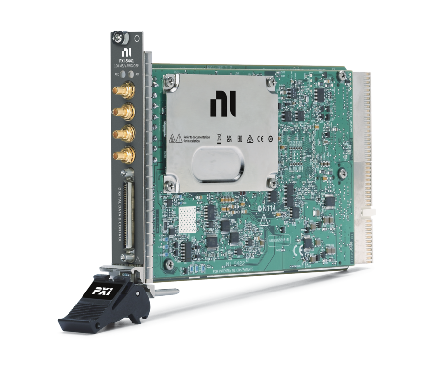
43 MHz带宽、16位、板载信号处理PXI波形发生器
ONETEST 欢迎您
厂商登录 | 入驻
登录 | 注册 购物车 微信公众号厂商登录
最大带宽:43 MHz
输出通道数量:1
模拟输出电压范围:-6 V 至 6 V
模拟输出分辨率:16 bits
43 MHz带宽、16位、板载信号处理PXI波形发生器
以下指标取自 Teledyne 官方在线规格书,按原文档小节分组。
| Number of channels | 1 |
| Connector | SMB (jack) |
| Direct | 50 Ω |
| 1 kΩ | 1.35 |
| Open | 1.41 |
| Low-Gain Amplifier | 50 Ω |
| 1 kΩ | 0.0107 |
| Open | 0.0113 |
| High-Gain Amplifier | 50 Ω |
| 1 kΩ | 0.0644 |
| Open | 0.0676 |
| Amplitude resolution | <0.06% (0.004 dB) of amplitude range |
| Offset range | Span of ±25% of the amplitude range with increments <0.0014% of amplitude range[2] |
| Direct | 50 Ω |
| 1 kΩ | ±0.953 |
| Open | ±1.000 |
| Low-Gain Amplifier | 50 Ω |
| 1 kΩ | ±1.905 |
| Open | ±2.000 |
| High-Gain Amplifier | 50 Ω |
| 1 kΩ | ±11.43 |
| Open | ±12.00 |
| DC Accuracy[4] Low-Gain or High-Gain Amplifier path ±0.2% of amplitude range ±0.05% of offset ±500 µV (within ±10 °C of self-calibration temperature) ±0.4% of amplitude range ±0.05% of offset ±1 mV (0 to 55 °C) Direct path Gain accuracy: ±0.2% amplitude range (within ±10 °C of self-calibration temperature) Gain accuracy: ±0.4% amplitude range (0 to 55 °C) DC error: ±30 mV (0 to 55 °C) | Low-Gain or High-Gain Amplifier path |
| Low-Gain or High-Gain Amplifier path | ±0.2% of amplitude range ±0.05% of offset ±500 µV (within ±10 °C of self-calibration temperature) ±0.4% of amplitude range ±0.05% of offset ±1 mV (0 to 55 °C) |
| Direct path | Gain accuracy: ±0.2% amplitude range (within ±10 °C of self-calibration temperature) Gain accuracy: ±0.4% amplitude range (0 to 55 °C) DC error: ±30 mV (0 to 55 °C) |
| AC amplitude accuracy[5] | (+2.0% + 1 mV), (-1.0% - 1 mV) (+0.8% + 0.5 mV), (-0.2% - 0.5 mV), typical |
| Output impedance | 50 Ω nominal or 75 Ω nominal, software-selectable |
| Load impedance compensation | Output amplitude is compensated for user-specified load impedances. |
| Output coupling | DC |
| Output enable | Software-selectable. When disabled, CH 0 output is terminated with a 1 W resistor with a value equal to the selected output impedance |
| Maximum output overload | The CH 0 output terminal can be connected to a 50 Ω, ±12 V (±8 V for the Direct path) source without sustaining any damage. No damage occurs if the CH 0 output is shorted to ground indefinitely. |
| Waveform summing | The CH 0 output supports waveform summing among similar paths-specifically, the output terminals of multiple PXI-5441 signal generators can be connected together. |
| Bandwidth[6] | 43 MHz |
| DAC digital interpolation filter[7] | Software-selectable finite impulse response (FIR) filter. Available interpolation factors are 2, 4, or 8. |
| Analog filter[8] | Software-selectable 7-pole elliptical filter for image suppression. |
| Passband flatness[9] Direct path -0.4 to +0.6 dB (100 Hz to 40 MHz) Low-gain amplifier path -1.0 to +0.5 dB (100 Hz to 20 MHz) High-gain amplifier path -1.2 to +0.5 dB (100 Hz to 20 MHz) | Direct path |
| Direct path | -0.4 to +0.6 dB (100 Hz to 40 MHz) |
| Low-gain amplifier path | -1.0 to +0.5 dB (100 Hz to 20 MHz) |
| High-gain amplifier path | -1.2 to +0.5 dB (100 Hz to 20 MHz) |
| Pulse response[10] Rise/fall time Direct path <5 ns <4.5 ns, typical[11] Low-gain amplifier path <8 ns <7 ns[11] <5.5 ns, typical[11] High-gain amplifier path <10 ns Aberration Direct path <10%, typical Low-gain amplifier path <5%, typical High-gain amplifier path <5%, typical | Rise/fall time Direct path <5 ns <4.5 ns, typical[11] Low-gain amplifier path <8 ns <7 ns[11] <5.5 ns, typical[11] High-gain amplifier path <10 ns |
| Rise/fall time Direct path <5 ns <4.5 ns, typical[11] Low-gain amplifier path <8 ns <7 ns[11] <5.5 ns, typical[11] High-gain amplifier path <10 ns | Direct path |
| Direct path | <5 ns <4.5 ns, typical[11] |
| Low-gain amplifier path | <8 ns <7 ns[11] <5.5 ns, typical[11] |
| High-gain amplifier path | <10 ns |
| Aberration Direct path <10%, typical Low-gain amplifier path <5%, typical High-gain amplifier path <5%, typical | Direct path |
| Direct path | <10%, typical |
| Low-gain amplifier path | <5%, typical |
| High-gain amplifier path | <5%, typical |
| Direct Sine 43 MHz Square Not recommended[14] Ramp Not recommended[14] Triangle Not recommended[14] | Sine |
| Sine | 43 MHz |
| Square | Not recommended[14] |
| Ramp | Not recommended[14] |
| Triangle | Not recommended[14] |
| Low-Gain Amplifier Sine 43 MHz Square 25 MHz Ramp 5 MHz Triangle 5 MHz | Sine |
| Sine | 43 MHz |
| Square | 25 MHz |
| Ramp | 5 MHz |
| Triangle | 5 MHz |
| High-Gain Amplifier Sine 43 MHz Square 12.5 MHz Ramp 5 MHz Triangle 5 MHz | Sine |
| Sine | 43 MHz |
| Square | 12.5 MHz |
| Ramp | 5 MHz |
| Triangle | 5 MHz |
| 1 | 64 |
| 10 | 61 |
| 20 | 57 |
| 30 | 60 |
| 40 | 60 |
| 43 | 58 |
| 1 | 76 |
| 10 | 68 |
| 20 | 60 |
| 30 | 73 |
| 40 | 76 |
| 43 | 78 |
| 1 | 87 |
| 10 | 86 |
| 20 | 79 |
| 30 | 72 |
| 40 | 75 |
| 43 | 77 |
| 20 kHz | -77, typical |
| 1 MHz | -75, typical |
| 5 MHz | -68 |
| 10 MHz | -65 -66, typical[20] |
| 20 MHz | -55 -61, typical[20] |
| 30 MHz | -50 -57, typical[20] |
| 40 MHz | -47 -54, typical[20] |
| 43 MHz | -46 -53, typical[20] |
| 20 kHz | -76, typical |
| 1 MHz | -74, typical |
| 5 MHz | -67 |
| 10 MHz | -63 |
| 20 MHz | -54 -57[20] |
| 30 MHz | -48 -52[20] |
| 40 MHz | -45 -50[20] |
| 43 MHz | -44 -49[20] |
| Direct | 1 |
| Low Gain | 0.06 |
| 0.1 | -16.0 |
| 0.4 | -4.0 |
| 1 | 4.0 |
| 2 | 10.0 |
| Divide-by-N | 23.84 S/s to 100 MS/s |
| High Resolution | 10 S/s to 100 MS/s |
| CLK IN | 200 kS/s to 105 MS/s |
| DDC CLK IN | 10 S/s to 105 MS/s |
| PXI Star Trigger | 10 S/s to 105 MS/s |
| PXI_Trig<0..7> | 10 S/s to 20 MS/s |
| 10 S/s to 105 MS/s | 1 (off) |
| 12.5 MS/s to 105 MS/s | 2 |
| 10 MS/s to 100 MS/s | 4 |
| 10 MS/s to 50 MS/s | 8 |
| Divide-by-N | ±1 Sample clock period |
| High-Resolution | ±1 Sample clock period |
| External (all) | 0 to 7.6 ns |
| Divide-by-N | -110 |
| High-Resolution[25] | -114 |
| CLK IN | -113 |
| PXI Star Trigger[26] | -115 |
| External Sample Clock Input Jitter Tolerance Cycle-cycle jitter ±300 ps Period Jitter ±1 ns | Cycle-cycle jitter |
| Cycle-cycle jitter | ±300 ps |
| Period Jitter | ±1 ns |
| Exported Sample Clock Destinations[27] | PFI<0..1> (SMB front panel connectors) DDC CLK OUT (DIGITAL DATA & CONTROL front panel connector) PXI_Trig<0..6> (PXI backplane connector) |
| PFI<0..1> | 105 MHz |
| DDC CLK OUT | 105 MHz |
| PXI_Trig<0..6> | 20 MHz |
| Clock Source | Internal sample clocks can either be locked to a reference clock using a phase-locked loop or be derived from the onboard VCXO frequency reference. |
| Frequency Accuracy | ±25 ppm |
| Reference Clock Sources[28] | PXI_CLK10 (PXI backplane connector) CLK IN (SMB front panel connector) |
| Frequency Accuracy | When using the PLL, the frequency accuracy of the PXI-5441 is solely dependent on the frequency accuracy of the PLL reference clock source. |
| Lock Time | 70 ms, typical 200 ms, maximum |
| Frequency Range | 5 to 20 MHz in increments of 1 MHz. Default of 10 MHz. The PLL reference clock frequency must be accurate to ±50 ppm. |
| Duty Cycle Range | 40 to 60% |
| Exported PLL Reference Clock Destinations | PFI<0..1> (SMB front panel connectors) PXI_Trig<0..6> (PXI backplane connector) |
| Connector | SMB (jack) |
| Direction | Input |
| Destinations | Sample clock PLL reference clock |
| Frequency Range | 1 to 105 MHz (sample clock destination and sine waves) 200 kHz to 105 MHz (sample clock destination and square waves) 5 to 20 MHz (PLL reference clock destination) |
| Input Voltage Range | Sine wave: 0.65 to 2.8 Vpk-pk into 50 Ω (0 dBm to +13 dBm) Square wave: 0.2 to 2.8 Vpk-pk into 50 Ω |
| Maximum Input Overload | ±10 V |
| Input Impedance | 50 Ω |
| Input Coupling | AC |
| Skew[29] | 500 ps, typical |
| Average skew after manual adjustment[30] | <10 ps, typical |
| Sample Clock delay/adjustment resolution | ≤10 ps, typical |
| Connectors | Two SMB (jacks) |
| Direction | Bidirectional |
| Frequency Range | DC to 105 MHz |
| Destinations | Start trigger |
| Maximum Input Overload | -2 to +7 V |
| VIH | 2.0 V |
| VIL | 0.8 V |
| Input Impedance | 1 kΩ |
| Sources | Sample clock divided by integer K (1 ≤ K ≤ 4,194,304) Sample clock timebase (100 MHz) divided by integer M (2 ≤ M ≤ 4,194,304) PLL reference clock Marker Exported start trigger (Out Start trigger) |
| Output Impedance | 50 Ω |
| Maximum Output Overload | -2 to +7 V |
| VOH[31] | Minimum: 2.9 V (open load), 1.4 V (50 Ω load) |
| VOL[31] | Maximum: 0.2 V (open load), 0.2 V (50 Ω load) |
| Rise/Fall Time[32] | ≤2.0 ns |
| Connector type | 68-pin VHDCI female receptacle |
| Number of Data Output Signals | 16 |
| Control signals | DDC CLK OUT (clock output) DDC CLK IN (clock input) PFI 2 (input) PFI 3 (input) PFI 4 (output) PFI 5 (output) |
| Ground | 23 pins |
| LVDS (Low-Voltage Differential Signal)[33] VOH 1.3 V, typical 1.7 V, maximum VOL 0.8 V, minimum 1.0 V , typical Differential Output Voltage 0.25 V , minimum 0.45 V , maximum Output Common-Mode Voltage 1.125 V , minimum 1.375 V , maximum Differential Pulse Skew (skew within a differential pair) 0.6 ns , maximum Rise/Fall time 0.5 ns , typical 1.6 ns , maximum | VOH |
| VOH | 1.3 V, typical 1.7 V, maximum |
| VOL | 0.8 V, minimum 1.0 V , typical |
| Differential Output Voltage | 0.25 V , minimum 0.45 V , maximum |
| Output Common-Mode Voltage | 1.125 V , minimum 1.375 V , maximum |
| Differential Pulse Skew (skew within a differential pair) | 0.6 ns , maximum |
| Rise/Fall time | 0.5 ns , typical 1.6 ns , maximum |
| Output skew | Typical: 1 ns; maximum 2 ns. Skew between any two output terminals on the DIGITAL DATA & CONTROL front panel connector. |
| Output Enable/Disable | Controlled through the software on all data output signals and control signals collectively. When disabled, the output terminals go to a high-impedance state. |
| Maximum Output Overload | -0.3 to +3.9 V |
| Signal type | LVDS (Low-Voltage Differential Signal) |
| Input Differential Impedance | 100 Ω |
| Maximum Output Overload | -0.3 to +3.9 V |
| Signal Characteristics Differential Input Voltage 0.1 V, minimum 0.5 V, maximum Input Common Mode Voltage 0.2 V, minimum 2.2 V, maximum | Differential Input Voltage |
| Differential Input Voltage | 0.1 V, minimum 0.5 V, maximum |
| Input Common Mode Voltage | 0.2 V, minimum 2.2 V, maximum |
| Clocking format | Data outputs and markers change on the falling edge of DDC CLK OUT. |
| Frequency Range | Refer to the Sample Clock section for more information |
| Duty cycle | 40 to 60% |
| Jitter | 40 ps rms |
| Clocking format | DDC data output signals change on the rising edge of DDC CLK IN. |
| Frequency range | 10 Hz to 105 MHz |
| Input Duty Cycle Tolerance | 40 to 60% |
| Input Jitter Tolerances | 300 ps pk-pk of cycle-cycle jitter, and 1 ns rms of period jitter. |
| Sources | PFI<0..1> (SMB front panel connectors) PFI<2..3> (DIGITAL DATA & CONTROL front panel connector) PXI_Trig<0..7> (backplane connector) PXI Star trigger (backplane connector) Software (use function call) Immediate (does not wait for a trigger). Default. |
| Modes | Single Continuous Stepped Burst |
| Edge Detection | Rising |
| Minimum Pulse Width | 25 ns |
| Digital interpolation filter disabled | 44 Sample clock periods + 110 ns |
| 2 | 58 Sample clock periods + 110 ns |
| 4 | 64 Sample clock periods + 110 ns |
| 8 | 65 Sample clock periods + 110 ns |
| Delay from Start Trigger to Digital Data Output with OSP Disabled. | 40 Sample clock periods + 110 ns |
| Additional Delay for Function Generator Mode | Add 33 Sample clock periods. (Applicable to delay from Start trigger to CH0 analog output and delay from Start trigger to digital data output) |
| Additional Delay with OSP Enabled[34] | Add 70 Sample clock periods for real data processing mode Add 73 Sample clock periods for complex data processing mode. (Applicable to delay from Start trigger to CH0 analog output and delay from Start trigger to digital data output) |
| Exported Trigger Destinations | A signal used as a trigger can be routed out to any destination listed in the Destinations specification in the Markers section. |
官方规格书:https://www.ni.com/docs/en-US/bundle/pxi-5441-specs/page/specs.html
NI官方渠道
官方渠道(官网 / 热线 / 邮箱)
官方渠道(中国大陆)
• 官网 www.ni.com/zh-cn
• 在线选购 www.ni.com/zh-cn/shop.html
• 经销商查询
官网「查找经销商」 www.ni.com/zh-cn/shop/advisors.html
• 联系方式
NI 中文官网不公布中国区电话与邮箱,报价、技术支持、校准、维修一律通过官网在线表单提交(「联系我们」页)
全国办事处
公司总部
• NI(National Instruments)
• 地址
11500 N Mopac Expwy, Austin, TX 78759-3504, United States
• 母公司
Emerson(2023 年完成收购,NI 隶属艾默生测试与测量业务集团)
0条提问
X
提问
X
回答
发表口碑

AI问答




 粤公网安备44030902003758