

 客服




总线连接:PXI Express
模拟输入阻抗:50 欧姆
示波器最大带宽:100 MHz
最大采样率:250 MS/s
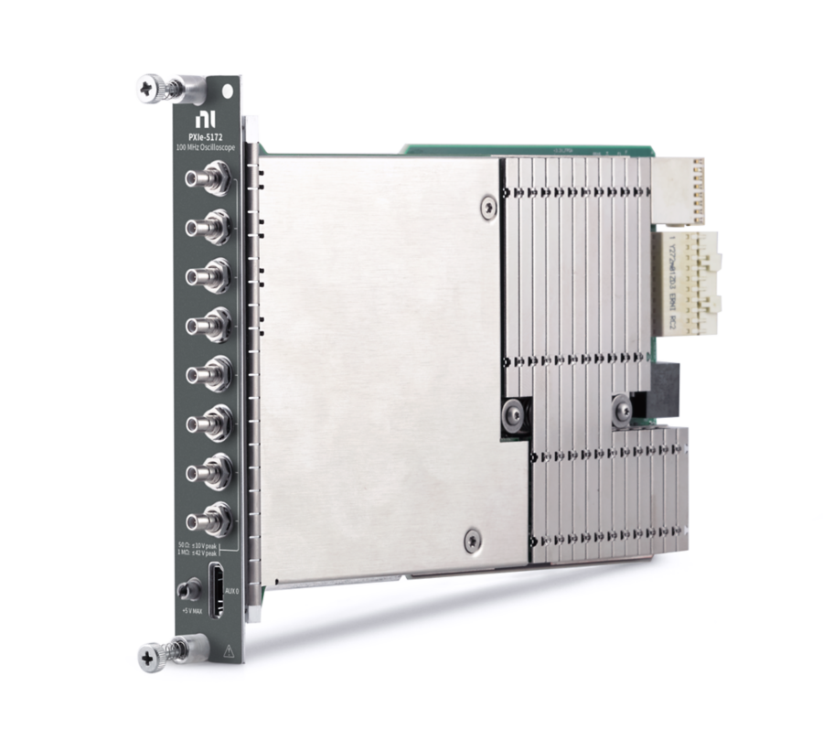
PXIe,100 MHz,4或8通道,14位,Kintex-7 325T或410T FPGA可重配置PXI示波器
ONETEST 欢迎您
厂商登录 | 入驻
登录 | 注册 购物车 微信公众号厂商登录
总线连接:PXI Express
模拟输入阻抗:50 欧姆
示波器最大带宽:100 MHz
最大采样率:250 MS/s
PXIe,100 MHz,4或8通道,14位,Kintex-7 325T或410T FPGA可重配置PXI示波器
以下指标取自 Teledyne 官方在线规格书,按原文档小节分组。
| CH 0 through CH 7 | SMB |
| AUX 0 | MHDMR |
| 1 | GND |
| 2 | CLK IN |
| 3 | GND |
| 4 | GND |
| 5 | CLK OUT |
| 6 | GND |
| 7 | GND |
| 8 | AUX 0/PFI 0 |
| 9 | AUX 0/PFI 1 |
| 10 | GND |
| 11 | AUX 0/PFI 2 |
| 12 | AUX 0/PFI 3 |
| 13 | GND |
| 14 | AUX 0/PFI 4 |
| 15 | AUX 0/PFI 5 |
| 16 | AUX 0/PFI 6 |
| 17 | AUX 0/PFI 7 |
| 18 | +3.3 V |
| 19 | GND |
| 1 | PFI 0 |
| 2 | PFI 1 |
| 3 | PFI 2 |
| 4 | PFI 3 |
| 5 | NC |
| 6 | CLK IN |
| 7 | NC |
| 8 | CLK OUT |
| 9 | PFI 4 |
| 10 | PFI 5 |
| 11 | PFI 6 |
| 12 | PFI 7 |
| 13 | +3.3 V |
| 14 to 26 | GND |
| CLK IN | BNC female |
| CLK OUT | Used to export the reference clock |
| PFI 0 | Bidirectional PFI line |
| PFI 1 | Bidirectional PFI line |
| PFI 2 | Bidirectional PFI line |
| PFI 3 | Bidirectional PFI line |
| Number of channels PXIe-5172 (4 CH) Four (simultaneously sampled) PXIe-5172 (8 CH) Eight (simultaneously sampled) | PXIe-5172 (4 CH) |
| PXIe-5172 (4 CH) | Four (simultaneously sampled) |
| PXIe-5172 (8 CH) | Eight (simultaneously sampled) |
| Input type | Referenced single-ended |
| Connectors | SMB, ground referenced |
| Input impedance | 50 Ω ±1.5%, typical 1 MΩ ±0.5%, typical |
| Input capacitance (1 MΩ) | 16 pF ±1.2 pF, typical |
| Input coupling | AC DC |
| 0.2 V | ±0.5 |
| 0.7 V | ±0.5 |
| 1.4 V | ±0.5 |
| 5 V | ±2.5 |
| 10 V [3] | 0 |
| 0.2 V | ±0.5 |
| 0.7 V | ±0.5 |
| 1.4 V | ±0.5 |
| 5 V | ±4.5 |
| 10 V | ±4.5 |
| 40 V | ±20 |
| 80 V | 0 |
| Maximum input overload 50 Ω 7 V RMS with |Peaks| ≤10 V 1 MΩ |Peaks| ≤42 V | 50 Ω |
| 50 Ω | 7 V RMS with |Peaks| ≤10 V |
| 1 MΩ | |Peaks| ≤42 V |
| Resolution | 14 bits |
| DC accuracy[4] 50 Ω ±[(0.45% × |Reading - Vertical Offset|) + (0.4% × |Vertical Offset|) + (0.05% of FS) + 0.4 mV], warranted 1 MΩ, 40 Vpk-pk range ±[(0.45% × |Reading - Vertical Offset|) + (0.5% × |Vertical Offset|) + (0.05% of FS) + 0.4 mV], warranted 1 MΩ, all other ranges ±[(0.45% × |Reading - Vertical Offset|) + (0.4% × |Vertical Offset|) + (0.05% of FS) + 0.4 mV], warranted | 50 Ω |
| 50 Ω | ±[(0.45% × |Reading - Vertical Offset|) + (0.4% × |Vertical Offset|) + (0.05% of FS) + 0.4 mV], warranted |
| 1 MΩ, 40 Vpk-pk range | ±[(0.45% × |Reading - Vertical Offset|) + (0.5% × |Vertical Offset|) + (0.05% of FS) + 0.4 mV], warranted |
| 1 MΩ, all other ranges | ±[(0.45% × |Reading - Vertical Offset|) + (0.4% × |Vertical Offset|) + (0.05% of FS) + 0.4 mV], warranted |
| DC drift[5] | ±[(0.010% × |Reading - Vertical Offset|) + (0.003% × |Vertical Offset|) + (0.006% of FS)] per °C |
| AC amplitude accuracy[4] 50 Ω ±0.15 dB at 50 kHz, warranted 1 MΩ, 40 Vpk-pk and 80 Vpk-pk ranges ±0.25 dB at 50 kHz, warranted 1 MΩ, all other ranges ±0.15 dB at 50 kHz, warranted | 50 Ω |
| 50 Ω | ±0.15 dB at 50 kHz, warranted |
| 1 MΩ, 40 Vpk-pk and 80 Vpk-pk ranges | ±0.25 dB at 50 kHz, warranted |
| 1 MΩ, all other ranges | ±0.15 dB at 50 kHz, warranted |
| Conversion error rate[6] 250 MS/sec <1 × 10⁻¹⁰ 200 MS/sec <1 × 10-15 150 MS/sec <1 × 10-20 | 250 MS/sec |
| 250 MS/sec | <1 × 10⁻¹⁰ |
| 200 MS/sec | <1 × 10-15 |
| 150 MS/sec | <1 × 10-20 |
| 1 MHz | -75 dB |
| 50 MHz | -75 dB |
| 100 MHz | -70 dB |
| 50 Ω | 0.2 V |
| All other input ranges | 100 MHz |
| 1 MΩ [9] | All input ranges |
| Bandwidth-limiting filters (digital FIR)[8],[10] | 20 MHz noise filter 40 MHz noise filter 80 MHz noise filter[11] |
| AC-coupling cutoff (-3 dB)[12] | 16.50 Hz |
| Rise/fall time[13] 50 Ω 5.15 ns 1 MΩ 5.25 ns | 50 Ω |
| 50 Ω | 5.15 ns |
| 1 MΩ | 5.25 ns |
| 0.2 V | -70 dBc |
| 0.7 V | -78 dBc |
| 1.4 V | -71 dBc |
| 5 V | -80 dBc |
| 0.2 V | -74 dBc |
| 0.7 V | -77 dBc |
| 1.4 V | -70 dBc |
| 5 V | -77 dBc |
| 0.2 V | 9.8 |
| 0.7 V | 11.4 |
| 1.4 V | 11.9 |
| 5 V | 11.8 |
| 0.2 V | 0.045 |
| All other input ranges | 0.018 |
| Sources Internal Onboard clock (internal VCXO) External AUX 0 CLK IN (front panel MHDMR connector) PXIe_DStarA (backplane connector) | Internal |
| Internal | Onboard clock (internal VCXO) |
| External | AUX 0 CLK IN (front panel MHDMR connector) PXIe_DStarA (backplane connector) |
| Sample rate range, real-time[17] | 3.815 kS/s to 250 MS/s |
| Sample clock jitter[18] | 700 fs RMS |
| Timebase frequency Internal (software-selectable) 250 MHz 200 MHz 150 MHz External 150 MHz to 250 MHz | Internal (software-selectable) |
| Internal (software-selectable) | 250 MHz 200 MHz 150 MHz |
| External | 150 MHz to 250 MHz |
| Timebase accuracy Phase-locked to onboard clock ±25 ppm, warranted Phase-locked to external clock Equal to the external clock accuracy | Phase-locked to onboard clock |
| Phase-locked to onboard clock | ±25 ppm, warranted |
| Phase-locked to external clock | Equal to the external clock accuracy |
| DC accuracy sampling drift, ±(% of |Reading|) per MHz from 250 MHz[19] | ±0.0127 |
| Duty cycle tolerance | 45% to 55% |
| Sources Internal None (internal VCXO) Onboard clock (internal VCXO) PXI_Clk10 (backplane connector) External (10 MHz)[20] AUX 0 CLK IN (front panel MHDMR connector) | Internal |
| Internal | None (internal VCXO) Onboard clock (internal VCXO) PXI_Clk10 (backplane connector) |
| External (10 MHz)[20] | AUX 0 CLK IN (front panel MHDMR connector) |
| Duty cycle tolerance | 45% to 55% |
| Source | AUX 0 CLK IN (front panel MHDMR connector) |
| Impedance | 50 Ω |
| Coupling | AC |
| Input voltage range As a 250 MHz sine wave 1 dBm through 18 dBm As a fast slew rate input (square wave, Vpk-pk) 0.4 V to 5 V | As a 250 MHz sine wave |
| As a 250 MHz sine wave | 1 dBm through 18 dBm |
| As a fast slew rate input (square wave, Vpk-pk) | 0.4 V to 5 V |
| Maximum input overload As a 250 MHz sine wave 20 dBm As a fast slew rate input (square wave, Vpk-pk) 6 V | As a 250 MHz sine wave |
| As a 250 MHz sine wave | 20 dBm |
| As a fast slew rate input (square wave, Vpk-pk) | 6 V |
| Source | AUX 0 CLK IN (front panel MHDMR connector) |
| Impedance | 50 Ω |
| Coupling | AC |
| Frequency[21] | 10 MHz |
| Input voltage range As a 250 MHz sine wave 1 dBm through 18 dBm As a fast slew rate input (square wave, Vpk-pk) 6 V | As a 250 MHz sine wave |
| As a 250 MHz sine wave | 1 dBm through 18 dBm |
| As a fast slew rate input (square wave, Vpk-pk) | 6 V |
| Duty cycle tolerance | 45% to 55% |
| Source | PXI_Clk10 (backplane connector) |
| Destination | AUX 0 CLK OUT |
| Output impedance | 50 Ω |
| Logic type | 3.3 V LVCMOS |
| Maximum current drive | ±8 mA |
| Source | System timing slot |
| Destinations | Onboard clock (internal VCXO) FPGA |
| Source | PXI backplane |
| Destination | Reference clock |
| Source | PXI backplane |
| Destination | FPGA |
| Supported triggers | Reference (stop) trigger Reference (arm) trigger Start trigger Advance trigger |
| Trigger types | Edge Hysteresis Window Digital Immediate Software |
| Dead time | Sample clock period × 10 |
| Holdoff | From Dead time to [(264 - 1) × Sample clock period] |
| Delay | From 0 to [(251 - 1) × Sample clock period] |
| Sources PXIe-5172 (4 CH) CH <0..3> PXIe-5172 (8 CH) CH <0..7> | PXIe-5172 (4 CH) |
| PXIe-5172 (4 CH) | CH <0..3> |
| PXIe-5172 (8 CH) | CH <0..7> |
| Enabled | Sample clock period / 1024 |
| Disabled | Sample clock period |
| Trigger accuracy[22] Input range (Vpk-pk): 0.2 V 0.75% of FS Input range (Vpk-pk): 0.7 V, 1.4 V, 5 V 0.5% of FS | Input range (Vpk-pk): 0.2 V |
| Input range (Vpk-pk): 0.2 V | 0.75% of FS |
| Input range (Vpk-pk): 0.7 V, 1.4 V, 5 V | 0.5% of FS |
| Trigger jitter[22] | 15 ps RMS |
| Minimum threshold duration[23] | Sample clock period |
| Sources | AUX 0 PFI <0..7> PXI_Trig <0..6> |
| Time resolution | Sample clock period × 2 |
| Rearm time | Sample clock period × 84 |
| Approximate trigger delay difference between analog edge trigger and digital trigger source[24] | 630 ns, nominal |
| Destinations | Reference (stop) trigger Reference (arm) trigger Start trigger Advance trigger |
| Time resolution | Sample clock period × 2 |
| Rearm time | Sample clock period × 84 |
| Connector | AUX 0 PFI <0..7> (front panel MHDMR connector) |
| Direction | Bidirectional per channel |
| Direction control latency | 125 ns |
| As an input (trigger) Destinations FPGA diagram Start trigger (acquisition arm) Reference (stop) trigger Arm Reference trigger Advance trigger Input impedance 49.9 kΩ VIH 2 V VIL 0.8 V Maximum input overload 0 V to 3.3 V (5 V tolerant) Minimum pulse width 10 ns | Destinations |
| Destinations | FPGA diagram Start trigger (acquisition arm) Reference (stop) trigger Arm Reference trigger Advance trigger |
| Input impedance | 49.9 kΩ |
| VIH | 2 V |
| VIL | 0.8 V |
| Maximum input overload | 0 V to 3.3 V (5 V tolerant) |
| Minimum pulse width | 10 ns |
| As an output (event) Sources FPGA diagram Ready for Start Start trigger (acquisition arm) Ready for Reference Reference (stop) trigger End of Record Ready for Advance Advance trigger Done (End of Acquisition) Output impedance 50 Ω Logic type 3.3 V CMOS Maximum current drive 12 mA Minimum pulse width 10 ns | Sources |
| Sources | FPGA diagram Ready for Start Start trigger (acquisition arm) Ready for Reference Reference (stop) trigger End of Record Ready for Advance Advance trigger Done (End of Acquisition) |
| Output impedance | 50 Ω |
| Logic type | 3.3 V CMOS |
| Maximum current drive | 12 mA |
| Minimum pulse width | 10 ns |
| Connector | AUX 0 +3.3 V (front panel MHDMR connector) |
| Voltage output | 3.3 V ±10% |
| Maximum current drive | 200 mA |
| Output impedance | <1 Ω |
| Onboard memory size[25] PXIe-5172 (4 CH) 0.75 GB PXIe-5172 (8 CH) 1.5 GB | PXIe-5172 (4 CH) |
| PXIe-5172 (4 CH) | 0.75 GB |
| PXIe-5172 (8 CH) | 1.5 GB |
| Minimum record length | 1 sample |
| Number of pretrigger samples | Zero up to (Record length - 1) |
| Number of posttrigger samples | Zero up to Record length |
| Maximum number of records in onboard memory | Total onboard memory / 48 × Number of channels, where number of channels is the number of channels enabled rounded up to the nearest power of two |
| FPGA support PXIe-5172 (4 CH) Xilinx Kintex-7 XC7K325T FPGA PXIe-5172 (8 CH) Xilinx Kintex-7 XC7K325T FPGA Xilinx Kintex-7 XC7K410T FPGA | PXIe-5172 (4 CH) |
| PXIe-5172 (4 CH) | Xilinx Kintex-7 XC7K325T FPGA |
| PXIe-5172 (8 CH) | Xilinx Kintex-7 XC7K325T FPGA Xilinx Kintex-7 XC7K410T FPGA |
官方规格书:https://www.ni.com/docs/en-US/bundle/pxie-5172-specs/page/specs.html
NI官方渠道
官方渠道(官网 / 热线 / 邮箱)
官方渠道(中国大陆)
• 官网 www.ni.com/zh-cn
• 在线选购 www.ni.com/zh-cn/shop.html
• 经销商查询
官网「查找经销商」 www.ni.com/zh-cn/shop/advisors.html
• 联系方式
NI 中文官网不公布中国区电话与邮箱,报价、技术支持、校准、维修一律通过官网在线表单提交(「联系我们」页)
全国办事处
公司总部
• NI(National Instruments)
• 地址
11500 N Mopac Expwy, Austin, TX 78759-3504, United States
• 母公司
Emerson(2023 年完成收购,NI 隶属艾默生测试与测量业务集团)
0条提问
X
提问
X
回答
发表口碑

AI问答




 粤公网安备44030902003758