

 客服




模拟输入耦合:直流
动态RAM(DRAM):4 GB
最大采样率:6.4 GS/s
模拟输入分辨率:12 bits
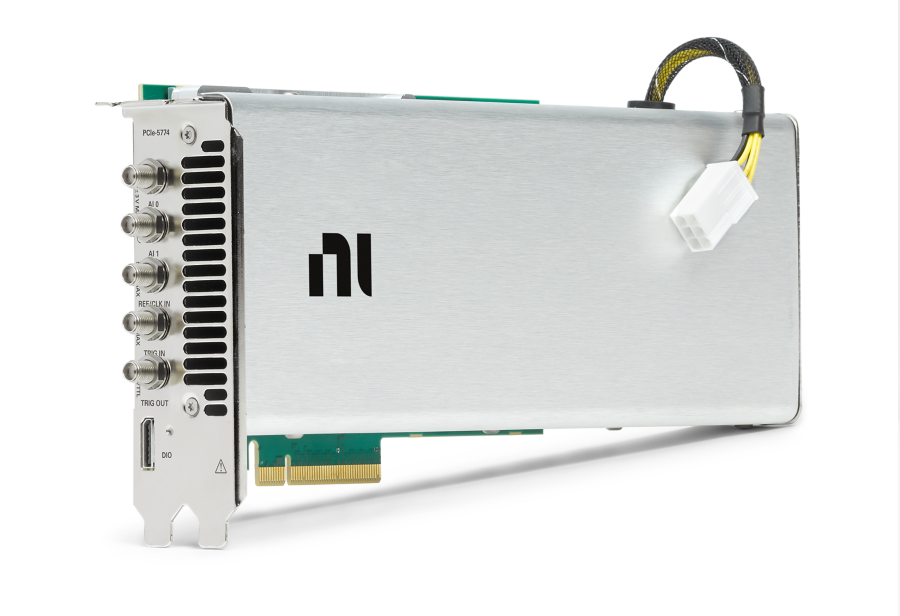
12位,6.4 GS/s,直流耦合,双通道PCI FlexRIO数字化设备
ONETEST 欢迎您
厂商登录 | 入驻
登录 | 注册 购物车 微信公众号厂商登录
模拟输入耦合:直流
动态RAM(DRAM):4 GB
最大采样率:6.4 GS/s
模拟输入分辨率:12 bits
12位,6.4 GS/s,直流耦合,双通道PCI FlexRIO数字化设备
以下指标取自 Teledyne 官方在线规格书,按原文档小节分组。
| Connector | Molex™ Nano-Pitch I/O™ |
| 5.0 V Power | ±5%, 50 mA maximum, nominal |
| MGT Tx± <0..3>* | Xilinx UltraScale GTH |
| MGT Rx± <0..3>* | Xilinx UltraScale GTH |
| DIO <0..7> | Single-ended |
| 5.0 V | DC |
| GND | Ground |
| Number of channels | 8 |
| Signal type | Single-ended |
| Voltage families | 3.3 V, 2.5 V, 1.8 V, 1.5 V, 1.2 V |
| Input impedance | 100 kΩ, nominal |
| Output impedance | 50 Ω, nominal |
| Direction control | Per channel |
| Minimum required direction change latency | 200 ns |
| Maximum output toggle rate | 60 MHz with 100 μA load, nominal |
| 3.3 | 0.8 |
| 2.5 | 0.7 |
| 1.8 | 0.62 |
| 1.5 | 0.51 |
| 1.2 | 0.42 |
| Data rate | 500 Mb/s to 16.375 Gb/s, nominal |
| Number of Tx channels | 4 |
| Number of Rx channels | 4 |
| I/O AC coupling capacitor | 100 nF |
| Minimum differential output voltage[2] | 170 mV peak-to-peak into 100 Ω, nominal |
| I/O coupling | AC-coupled, includes 100 nF capacitor |
| Differential input voltage range ≤ 6.6 Gb/s 150 mV peak-to-peak to 2000 mV peak-to-peak, nominal > 6.6 Gb/s 150 mV peak-to-peak to 1250 mV peak-to-peak, nominal | ≤ 6.6 Gb/s |
| ≤ 6.6 Gb/s | 150 mV peak-to-peak to 2000 mV peak-to-peak, nominal |
| > 6.6 Gb/s | 150 mV peak-to-peak to 1250 mV peak-to-peak, nominal |
| Differential input resistance | 100 Ω, nominal |
| I/O coupling | DC-coupled, requires external capacitor |
| LUTs | 203,128 |
| DSP48 slices (25 × 18 multiplier) | 1,700 |
| Embedded Block RAM | 19.0 Mb |
| Data Clock Domain | 200 MHz, 16 samples per cycle per channel (dual channel mode), 32 samples per cycle (single channel mode) |
| Timebase reference sources | Onboard 100 MHz oscillator |
| Data transfers | DMA, interrupts, programmed I/O |
| Number of DMA channels | 59 |
| Memory size | 4 GB (2 banks of 2 GB) |
| DRAM clock rate | 1064 MHz |
| Physical bus width | 32 bit |
| LabVIEW FPGA DRAM clock rate | 267 MHz |
| LabVIEW FPGA DRAM bus width | 256 bit per bank |
| Maximum theoretical data rate | 17 GB/s (8.5 GB/s per bank) |
| Number of channels | 2, single-ended, simultaneously sampled |
| Connector type | SMA |
| Input impedance | 50 Ω, nominal |
| Input coupling | DC |
| Sample Clock Internal Sample Clock[3] 3.2 GHz External Sample Clock[3] 3.2 GHz | Internal Sample Clock[3] |
| Internal Sample Clock[3] | 3.2 GHz |
| External Sample Clock[3] | 3.2 GHz |
| Sample Rate Dual channel mode 3.2 GS/s per channel Single channel mode 6.4 GS/s | Dual channel mode |
| Dual channel mode | 3.2 GS/s per channel |
| Single channel mode | 6.4 GS/s |
| Analog-to-digital converter (ADC) | ADC12DJ3200, 12-bit resolution |
| Full-scale input ranges | 200 mV peak-to-peak 1 V peak-to-peak |
| Gain accuracy 200 mV range ±1.47% 1 V range ±1.44% | 200 mV range |
| 200 mV range | ±1.47% |
| 1 V range | ±1.44% |
| DC offset 200 mV range ±0.628 mV 1 V range ±1.269 mV | 200 mV range |
| 200 mV range | ±0.628 mV |
| 1 V range | ±1.269 mV |
| Vertical offset range | ±0.5 full-scale, nominal |
| Bandwidth (-3 dB)[4] -01 variant 200 mV range: 3.00 GHz 1 V range: 2.85 GHz -02 variant 200 mV range: 1.63 GHz 1 V range: 1.62 GHz | -01 variant |
| -01 variant | 200 mV range: 3.00 GHz 1 V range: 2.85 GHz |
| -02 variant | 200 mV range: 1.63 GHz 1 V range: 1.62 GHz |
| SNR* (dBFS) | 54.7 |
| SINAD* (dBFS) | 54.4 |
| SFDR (dBc) | -65.2 |
| ENOB† (bits) | 8.7 |
| SNR* (dBFS) | 54.0 |
| SINAD* (dBFS) | 53.9 |
| SFDR (dBc) | -61.3 |
| ENOB† (bits) | 8.7 |
| SNR* (dBFS) | 52.0 |
| SINAD* (dBFS) | 51.9 |
| SFDR (dBc) | -65.1 |
| ENOB† (bits) | 8.3 |
| SNR* (dBFS) | 51.0 |
| SINAD* (dBFS) | 51.0 |
| SFDR (dBc) | -57.8 |
| ENOB† (bits) | 8.2 |
| Dual channel | 15.3 |
| Single channel | 10.2 |
| Dual channel | 4.3 |
| Single channel | 3.1 |
| Channel-to-channel crosstalk, measured 99.9 MHz -94.1 dB 399 MHz -85.6 dB 999 MHz -82.5 dB 1.59 GHz -75.6 dB 1.99 GHz -72.2 dB | 99.9 MHz |
| 99.9 MHz | -94.1 dB |
| 399 MHz | -85.6 dB |
| 999 MHz | -82.5 dB |
| 1.59 GHz | -75.6 dB |
| 1.99 GHz | -72.2 dB |
| Connector type | SMA |
| Input impedance | 50 Ω |
| Input coupling | AC |
| Input voltage range | 0.35 V peak-to-peak to 3.5 V peak-to-peak |
| Absolute maximum voltage | ±12 V DC, 5 V peak-to-peak AC |
| Duty cycle | 45% to 55% |
| Onboard reference timebase stability | ±0.7 ppm |
| Sample Clock jitter[5] | 85 fs RMS, measured |
| Internal Reference Clock* | — |
| Internal Baseboard Reference Clock | 10 MHz |
| External Reference Clock (REF/CLK IN) | 10 MHz† |
| External Sample Clock (REF/CLK IN) | 3.2 GHz |
| Connector type | SMA |
| Input impedance | 50 Ω, nominal |
| Input coupling | DC |
| Input voltage range | ±5 V |
| Comparator threshold resolution | 12 bits |
| Minimum pulse width | 5 ns |
| Absolute maximum voltage | ±6 V |
| Connector type | SMA |
| Input impedance | 50 Ω, nominal |
| Input coupling | DC |
| Logic type | 3.3 V CMOS |
| Maximum current drive | 24 mA |
| Update rate resolution | 5 ns |
| Jitter | 3.2 ps RMS, measured |
| Card edge form factor | PCI Express Gen-3 x8 |
| Slot compatibility | x8, and x16 PCI Express slots |
| +3.3 V | 4.5 A |
| +12 V | 5 A |
| Maximum total power | 75 W |
| Dimensions (including I/O bracket, not including connectors) | 12.6 cm × 26.3 cm × 4 cm (5.0 in. × 10.4 in. × 1.6 in.) |
| Weight | 990 g (35 oz) |
| PCI Express mechanical form factor | Standard height, three-quarter length, double slot |
| Integrated air mover (fan) | Yes |
| Maximum rear panel exhaust airflow | 84 m3/h (50 CFM) (without any chassis impedance) |
| Maximum altitude | 2,000 m (800 mbar) (at 25 °C ambient temperature) |
| Pollution Degree | 2 |
| Operating temperature, local[6] | 0 °C to 45 °C |
| Operating humidity | 10% to 90% RH, noncondensing |
| Ambient temperature range | -20 °C to 70 °C |
| Relative humidity range | 5% to 95% RH, noncondensing |
官方规格书:https://www.ni.com/docs/en-US/bundle/pcie-5774-specs/page/specs.html
NI官方渠道
官方渠道(官网 / 热线 / 邮箱)
官方渠道(中国大陆)
• 官网 www.ni.com/zh-cn
• 在线选购 www.ni.com/zh-cn/shop.html
• 经销商查询
官网「查找经销商」 www.ni.com/zh-cn/shop/advisors.html
• 联系方式
NI 中文官网不公布中国区电话与邮箱,报价、技术支持、校准、维修一律通过官网在线表单提交(「联系我们」页)
全国办事处
公司总部
• NI(National Instruments)
• 地址
11500 N Mopac Expwy, Austin, TX 78759-3504, United States
• 母公司
Emerson(2023 年完成收购,NI 隶属艾默生测试与测量业务集团)
0条提问
X
提问
X
回答
发表口碑

AI问答




 粤公网安备44030902003758