

 客服




双向数字通道数量:32
逻辑电平和范围:Programmable
信令类型:单端
最大信号生成速率:400 Mbits/s
PXIe,200 MHz,32通道PXI数字波形仪器
ONETEST 欢迎您
厂商登录 | 入驻
登录 | 注册 购物车 微信公众号厂商登录
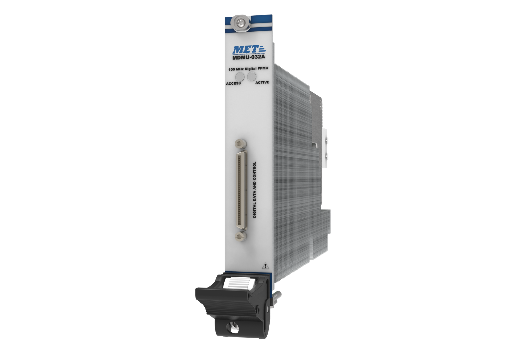
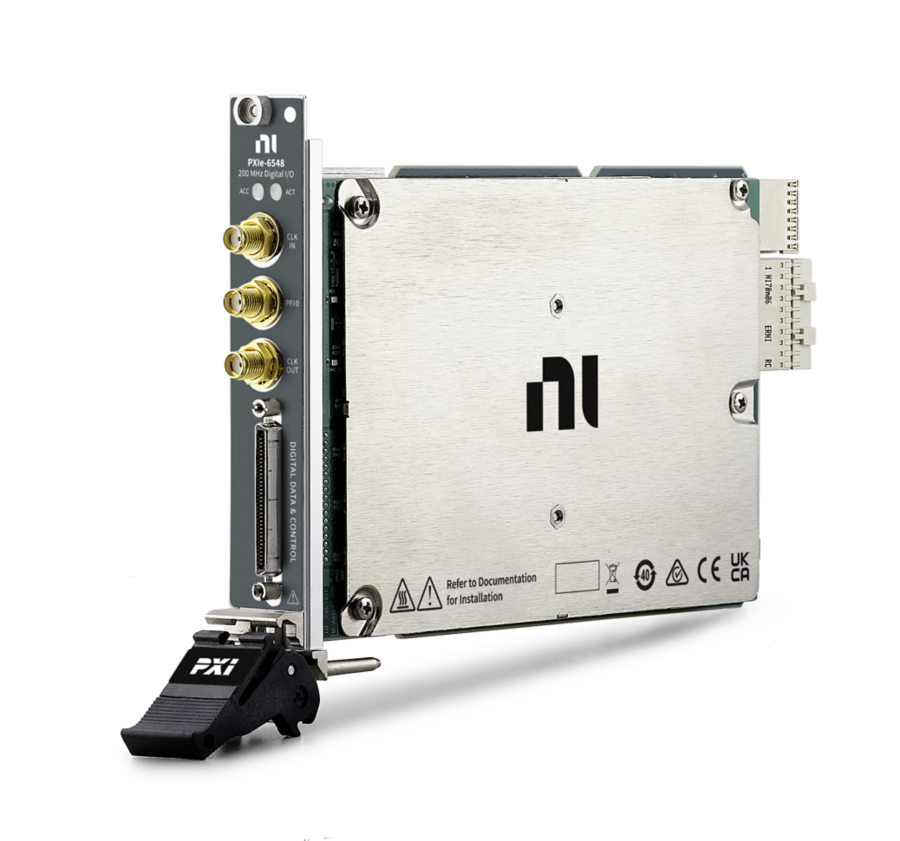
双向数字通道数量:32
逻辑电平和范围:Programmable
信令类型:单端
最大信号生成速率:400 Mbits/s
PXIe,200 MHz,32通道PXI数字波形仪器
以下指标取自 Teledyne 官方在线规格书,按原文档小节分组。
| 33 | DDC_CLK OUT |
| 67 | Strobe |
| 1, 3, 5, 7, 9, 11, 13, 15, 17, 19, 21, 23, 25, 27, 29, 31, 35, 37, 39, 41, 43, 45, 47, 49, 51, 53, 55, 57, 59, 61, 63, 65 | DIO <0..31> |
| 26, 30, 64 | Programmable Function Interface (PFI) <1..3> |
| 2, 4, 6, 10, 12, 14, 16, 18, 20, 22, 24, 28, 32, 34, 36, 38, 40, 42, 44, 46, 48, 50, 54, 56, 58, 62, 66 | GND |
| 8, 52, 60 | RESERVED |
| CLK IN | Reference Clock Input |
| CLK OUT | Reference Clock Output |
| Data Number of channels SDR selected (data clocked using Sample clock rising or falling edge) 32 DDR selected (data clock using both Sample clock edges)[1] 16 per direction Extended data mode selected[2] 24 Direction control Per channel Per cycle | Number of channels SDR selected (data clocked using Sample clock rising or falling edge) 32 DDR selected (data clock using both Sample clock edges)[1] 16 per direction Extended data mode selected[2] 24 |
| Number of channels SDR selected (data clocked using Sample clock rising or falling edge) 32 DDR selected (data clock using both Sample clock edges)[1] 16 per direction Extended data mode selected[2] 24 | SDR selected (data clocked using Sample clock rising or falling edge) |
| SDR selected (data clocked using Sample clock rising or falling edge) | 32 |
| DDR selected (data clock using both Sample clock edges)[1] | 16 per direction |
| Extended data mode selected[2] | 24 |
| Direction control | Per channel Per cycle |
| Time to tristate (tPZ), 2 kΩ and 15 pF load | 6.2 ns, nominal |
| Programmable Function Interface (PFI) Number of channels 4 Direction control Per channel | Number of channels |
| Number of channels | 4 |
| Direction control | Per channel |
| Clock terminals Input 2 Output 2 | Input |
| Input | 2 |
| Output | 2 |
| Channels | Data DDC CLK OUT PFI <0..3> |
| Generation signal type | Single-ended |
| Generation voltage features, all Data, PFI, and clock channels Number of programmable generation voltage levels[3] 1 voltage high level (VOH) Generation voltage low level (VOL) is always set to 0 V Range 1.2 V to 3.3 V Resolution 100 mV | Number of programmable generation voltage levels[3] |
| Number of programmable generation voltage levels[3] | 1 voltage high level (VOH) Generation voltage low level (VOL) is always set to 0 V |
| Range | 1.2 V to 3.3 V |
| Resolution | 100 mV |
| DC generation voltage accuracy[4] | ±35 mV, typical ±200 mV, maximum |
| 1.2 V (VOH = 1.2 V) | 0.0 V |
| 1.5 V (VOH = 1.5 V) | 1.3 V |
| 1.8 V (VOH = 1.8 V) | 1.6 V |
| 2.5 V (VOH = 2.5 V) | 2.3 V |
| 3.3 V (VOH = 3.3 V) | 3.1 V |
| Output impedance | 50 Ω, nominal |
| Maximum allowed DC drive strength per channel, by logic family 1.2 V ±12 mA, nominal 1.5 V ±15 mA, nominal 1.8 V ±18 mA, nominal 2.5 V ±25 mA, nominal 3.3 V ±33 mA, nominal | 1.2 V |
| 1.2 V | ±12 mA, nominal |
| 1.5 V | ±15 mA, nominal |
| 1.8 V | ±18 mA, nominal |
| 2.5 V | ±25 mA, nominal |
| 3.3 V | ±33 mA, nominal |
| Data channel driver enable/disable control | Software-selectable: per channel |
| Channel power-on state | Drivers disabled, 50 kΩ nominal input impedance |
| Output protection Range 0 V to 5 V Duration Indefinite | Range |
| Range | 0 V to 5 V |
| Duration | Indefinite |
| Channels | Data STROBE PFI <0..3> |
| Acquisition signal type | Single-ended |
| Acquisition threshold features, all Data, PFI, and clock channels Number of programmable acquisition thresholds[6] 1 (VIH = VIL) Range 0.6 V to 1.65 V Resolution 50 mV | Number of programmable acquisition thresholds[6] |
| Number of programmable acquisition thresholds[6] | 1 (VIH = VIL) |
| Range | 0.6 V to 1.65 V |
| Resolution | 50 mV |
| Accuracy[7] | ±150 mV, typical ±30%, maximum |
| 1.2 V (VIH, VIL = 0.60 V) | 420 mV |
| 1.5 V (VIH, VIL = 0.75 V) | 525 mV |
| 1.8 V (VIH, VIL = 0.90 V) | 630 mV |
| 2.5 V (VIH, VIL = 1.25 V) | 875 mV |
| 3.3 V (VIH, VIL = 1.65 V) | 1.155 V |
| Input impedance | High-impedance (50 kΩ), nominal |
| Input protection[9] | -1 V to 5 V |
| Sources | 1. On Board clock (internal 800 MHz VCO with 32-bit DDS) 2. CLK IN (SMA jack connector) 3. STROBE (Digital Data & Control [DDC] connector; acquisition only) |
| Frequency range On Board clock 100 Hz to 200 MHz CLK IN 20 kHz to 200 MHz STROBE 100 Hz to 200 MHz | On Board clock |
| On Board clock | 100 Hz to 200 MHz |
| CLK IN | 20 kHz to 200 MHz |
| STROBE | 100 Hz to 200 MHz |
| On Board clock characteristics Resolution[10] 0.2 Hz, maximum Accuracy[11] ±150 ppm + 5 ppm per year On Board clock characteristics valid only when PLL reference source is set to None Frequency accuracy ±150 ppm (including temperature effects), typical Aging ±5 ppm first year, nominal | Resolution[10] |
| Resolution[10] | 0.2 Hz, maximum |
| Accuracy[11] | ±150 ppm + 5 ppm per year |
| On Board clock characteristics valid only when PLL reference source is set to None Frequency accuracy ±150 ppm (including temperature effects), typical Aging ±5 ppm first year, nominal | Frequency accuracy |
| Frequency accuracy | ±150 ppm (including temperature effects), typical |
| Aging | ±5 ppm first year, nominal |
| Sample clock relative delay adjustment[12] Range Acquisition sessions 0.0 to 1.0 Sample clock periods Generation sessions 0.0 ns to 5.0 ns Resolution 0.5 ps | Range Acquisition sessions 0.0 to 1.0 Sample clock periods Generation sessions 0.0 ns to 5.0 ns |
| Range Acquisition sessions 0.0 to 1.0 Sample clock periods Generation sessions 0.0 ns to 5.0 ns | Acquisition sessions |
| Acquisition sessions | 0.0 to 1.0 Sample clock periods |
| Generation sessions | 0.0 ns to 5.0 ns |
| Resolution | 0.5 ps |
| Exported Sample clock destinations | DDC CLK OUT (DDC connector) CLK OUT (SMA jack connector) |
| Exported Sample clock delay Range 0.0 to 1.0 Sample clock periods Resolution (δC)[13] 117 ps to 143 ps, nominal Frequency On Board clock All supported frequencies External clock Frequencies ≥20 MHz | Range |
| Range | 0.0 to 1.0 Sample clock periods |
| Resolution (δC)[13] | 117 ps to 143 ps, nominal |
| Frequency On Board clock All supported frequencies External clock Frequencies ≥20 MHz | On Board clock |
| On Board clock | All supported frequencies |
| External clock | Frequencies ≥20 MHz |
| Exported Sample clock jitter, using On Board clock Period 24 psrms, characteristic Cycle-to-cycle 43 psrms, characteristic | Period |
| Period | 24 psrms, characteristic |
| Cycle-to-cycle | 43 psrms, characteristic |
| Channels | Data DDC CLK OUT PFI <0..3> |
| Data channel-to-channel skew[14] | ±300 ps, maximum |
| 3.3 V | 200 Mbps |
| 2.5 V | 400 Mbps |
| 1.8 V | 375 Mbps |
| 1.5 V | 350 Mbps |
| 1.2 V | 300 Mbps |
| 2.5 V to 3.3 V | 200 Mbps |
| 1.8 V to 2.4 V | 375 Mbps |
| 1.5 V to 1.7 V | 350 Mbps |
| 1.2 V to 1.4 V | 300 Mbps |
| Data position modes | Sample clock rising edge Sample clock falling edge Delay from Sample clock rising edge |
| Data delay banks Bank 0 DIO <0..3> DIO <16..19> DIO <28..31> PFI <0..3> Bank 1 DIO <4..7> DIO <20..23> Bank 2 DIO <8..15> DIO <24..27> | Bank 0 |
| Bank 0 | DIO <0..3> DIO <16..19> DIO <28..31> PFI <0..3> |
| Bank 1 | DIO <4..7> DIO <20..23> |
| Bank 2 | DIO <8..15> DIO <24..27> |
| Generation data delay Range (δG) 0.0 to 1.0 Sample clock periods Resolution (δG)[18] 117 ps to 143 ps, nominal Generation data delay frequency On Board clock All supported frequencies External clock Frequencies ≥20 MHz | Range (δG) |
| Range (δG) | 0.0 to 1.0 Sample clock periods |
| Resolution (δG)[18] | 117 ps to 143 ps, nominal |
| Generation data delay frequency On Board clock All supported frequencies External clock Frequencies ≥20 MHz | On Board clock |
| On Board clock | All supported frequencies |
| External clock | Frequencies ≥20 MHz |
| Exported Sample clock offset (tCO)[19] | 0.0 ns or 1.65 ns (default), nominal |
| Time delay from On Board Sample clock to DDC connector (tSCDDC) | 8.1 ns, characteristic; exported Sample clock offset = 0 ns |
| 1.65 ns | tp - 2.15 ns |
| 0.0 ns | tp - 500 ps |
| Channels | Data STROBE PFI <0..3> |
| Channel-to-channel skew[20] | ±350 ps |
| 3.3 V | 200 Mbps |
| 2.5 V | 300 Mbps |
| 1.8 V | 250 Mbps |
| 1.5 V | 225 Mbps |
| 1.2 V | 200 Mbps |
| 1.25 V to 1.65 V | 200 Mbps |
| 0.90 V to 1.20 V | 250 Mbps |
| 0.75 V to 0.85 V | 225 Mbps |
| 0.60 V to 0.70 V | 200 Mbps |
| Data position modes | Sample clock rising edge Sample clock falling edge Delay from Sample clock rising edge |
| 1.25 V to 1.65 V | 2.8 ns |
| 0.90 V to 1.20 V | 1.20 ns |
| 0.75 V to 0.85 V | 1.40 ns |
| 0.60 V to 0.70 V | 1.75 ns |
| Setup and hold times to Sample clock[24] Setup time (tsusc) 900 ps, nominal Hold time (tHSC) 425 ps, nominal | Setup time (tsusc) |
| Setup time (tsusc) | 900 ps, nominal |
| Hold time (tHSC) | 425 ps, nominal |
| Data delay banks[25] Bank 0 DIO <0..3> DIO <16..19> DIO <28..31> PFI <0..3> Bank 1 DIO <4..7> DIO <20..23> Bank 2 DIO <8..15> DIO <24..27> | Bank 0 |
| Bank 0 | DIO <0..3> DIO <16..19> DIO <28..31> PFI <0..3> |
| Bank 1 | DIO <4..7> DIO <20..23> |
| Bank 2 | DIO <8..15> DIO <24..27> |
| Time delay from DDC connector to internal Sample clock | 6.8 ns, nominal |
| Acquisition data delay Frequency On Board clock All supported frequencies External clock and STROBE Frequencies ≥20 MHz Range 0.0 to 1.0 Sample clock periods Resolution[26] 117 ps to 143 ps, nominal | Frequency On Board clock All supported frequencies External clock and STROBE Frequencies ≥20 MHz |
| Frequency On Board clock All supported frequencies External clock and STROBE Frequencies ≥20 MHz | On Board clock |
| On Board clock | All supported frequencies |
| External clock and STROBE | Frequencies ≥20 MHz |
| Range | 0.0 to 1.0 Sample clock periods |
| Resolution[26] | 117 ps to 143 ps, nominal |
| Connector | SMA jack |
| Direction | Input |
| Destinations | 1. Reference clock (PLL) 2. Sample clock |
| Input coupling | AC |
| Input protection | ±10 VDC, nominal |
| Input impedance | Software-selectable: 50 Ω (default) or 1 kΩ, nominal |
| Minimum detectable pulse width | 2 ns, nominal |
| Clock requirements | Free-running (continuous) clock |
| Square wave voltage range | 0.65 Vpk-pk to 5.0 Vpk-pk |
| 0.65 to 5.0 | 20 MHz to 200 MHz |
| 1.0 to 5.0 | 13 MHz to 200 MHz |
| 1.3 to 5.0 | 10 MHz to 200 MHz |
| 2.6 to 5.0 | 5 MHz to 200 MHz |
| As Sample clock[27] Frequency range 20 kHz to 200 MHz Duty cycle range ƒ <20 MHz 25% to 75% ƒ ≥20 MHz 40% to 60% | Frequency range |
| Frequency range | 20 kHz to 200 MHz |
| Duty cycle range ƒ <20 MHz 25% to 75% ƒ ≥20 MHz 40% to 60% | ƒ <20 MHz |
| ƒ <20 MHz | 25% to 75% |
| ƒ ≥20 MHz | 40% to 60% |
| As Reference clock Frequency range 5 MHz to 100 MHz (integer multiples of 1 MHz) Frequency accuracy[28] ±0.1% Duty cycle range 25% to 75% | Frequency range |
| Frequency range | 5 MHz to 100 MHz (integer multiples of 1 MHz) |
| Frequency accuracy[28] | ±0.1% |
| Duty cycle range | 25% to 75% |
| Connector | DDC |
| Direction | Input |
| Destination | Sample clock (acquisition only) |
| Frequency range | 100 Hz to 200 MHz |
| Duty cycle range (at the programmed threshold) ƒ <20 MHz 25% to 75% ƒ ≥20 MHz 40% to 60% (corrected to 50%) | ƒ <20 MHz |
| ƒ <20 MHz | 25% to 75% |
| ƒ ≥20 MHz | 40% to 60% (corrected to 50%) |
| Minimum detectable pulse width[29] | 2 ns, nominal |
| Clock requirements | Free-running (continuous) clock |
| Input impedance | 50 kΩ, nominal |
| Connector | SMA jack |
| Direction | Output |
| Sources | 1. Sample clock (excluding STROBE) 2. Reference clock (PLL) |
| Output impedance | 50 Ω, nominal |
| Logic type | Matched with generation and acquisition sessions |
| Connector | DDC |
| Direction | Output |
| Source | Sample clock (generation only) |
| Sources[30] | 1. PXI_CLK100 (PXI Express backplane) 2. CLK IN (SMA jack connector) 3. None (internal oscillator locked to an internal reference) |
| Destination | CLK OUT (SMA jack connector) |
| Lock time | 150 ms, maximum (not including software latency) |
| Frequency range | 5 MHz to 100 MHz (integer multiples of 1 MHz), 0.1% required accuracy |
| Duty cycle range | 25% to 75% |
| Onboard memory size[31] 1 Mbit per channel Acquisition 1 Mbit per channel (4 MBytes total) Generation 1 Mbit per channel (4 MBytes total) 8 Mbit per channel Acquisition 8 Mbit per channel (32 MBytes total) Generation 8 Mbit per channel (32 MBytes total) 64 Mbit per channel Acquisition 64 Mbit per channel (256 MBytes total) Generation 64 Mbit per channel (256 MBytes total) | 1 Mbit per channel Acquisition 1 Mbit per channel (4 MBytes total) Generation 1 Mbit per channel (4 MBytes total) |
| 1 Mbit per channel Acquisition 1 Mbit per channel (4 MBytes total) Generation 1 Mbit per channel (4 MBytes total) | Acquisition |
| Acquisition | 1 Mbit per channel (4 MBytes total) |
| Generation | 1 Mbit per channel (4 MBytes total) |
| 8 Mbit per channel Acquisition 8 Mbit per channel (32 MBytes total) Generation 8 Mbit per channel (32 MBytes total) | Acquisition |
| Acquisition | 8 Mbit per channel (32 MBytes total) |
| Generation | 8 Mbit per channel (32 MBytes total) |
| 64 Mbit per channel Acquisition 64 Mbit per channel (256 MBytes total) Generation 64 Mbit per channel (256 MBytes total) | Acquisition |
| Acquisition | 64 Mbit per channel (256 MBytes total) |
| Generation | 64 Mbit per channel (256 MBytes total) |
| Generation Single-waveform mode Generates a single waveform once, n times, or continuously Scripted mode[32] Generates a simple or complex sequence of waveforms. Finite repeat count 1 to 16,777,216 Waveform quantum[33] Data width = 4 1 sample Data width = 2 2 samples Waveform block size (in physical memory) Data width = 4 32 samples Data width = 2 64 samples | Single-waveform mode |
| Single-waveform mode | Generates a single waveform once, n times, or continuously |
| Scripted mode[32] | Generates a simple or complex sequence of waveforms. |
| Finite repeat count | 1 to 16,777,216 |
官方规格书:https://www.ni.com/docs/en-US/bundle/pxie-6548-specs/page/specs.html
NI官方渠道
官方渠道(官网 / 热线 / 邮箱)
官方渠道(中国大陆)
• 官网 www.ni.com/zh-cn
• 在线选购 www.ni.com/zh-cn/shop.html
• 经销商查询
官网「查找经销商」 www.ni.com/zh-cn/shop/advisors.html
• 联系方式
NI 中文官网不公布中国区电话与邮箱,报价、技术支持、校准、维修一律通过官网在线表单提交(「联系我们」页)
全国办事处
公司总部
• NI(National Instruments)
• 地址
11500 N Mopac Expwy, Austin, TX 78759-3504, United States
• 母公司
Emerson(2023 年完成收购,NI 隶属艾默生测试与测量业务集团)
0条提问
X
提问
X
回答
发表口碑

AI问答




 粤公网安备44030902003758