

 客服



双向数字通道数量:24
逻辑电平和范围:Programmable
板载内存:8 Mbit/ch
信令类型:单端
200 MHz,24通道板载PPMU,PXI数字波形仪
ONETEST 欢迎您
厂商登录 | 入驻
登录 | 注册 购物车 微信公众号厂商登录
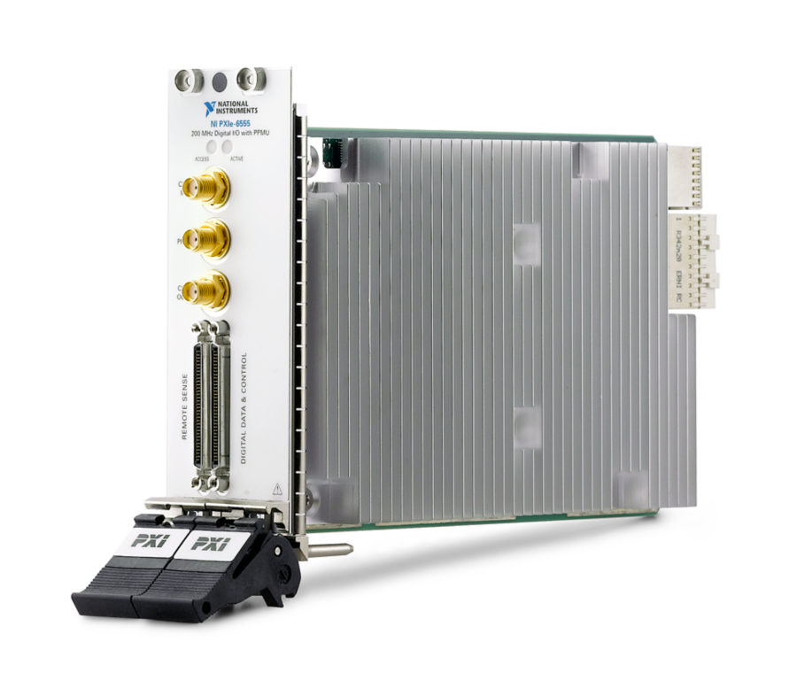
双向数字通道数量:24
逻辑电平和范围:Programmable
板载内存:8 Mbit/ch
信令类型:单端
200 MHz,24通道板载PPMU,PXI数字波形仪
以下指标取自 Teledyne 官方在线规格书,按原文档小节分组。
| Data Number of channels 24, per-pin parametric measurement unit (PPMU)–enabled Direction control Per channel | Number of channels |
| Number of channels | 24, per-pin parametric measurement unit (PPMU)–enabled |
| Direction control | Per channel |
| Programmable Function Interface (PFI) Number of channels PPMU-enabled: 4 PFI 1 PFI 2 PFI 4/DDC CLK OUT PFI 5/STROBE General: 10 PFI 0 PFI 3 PFI <24..31> Direction control Per channel | Number of channels PPMU-enabled: 4 PFI 1 PFI 2 PFI 4/DDC CLK OUT PFI 5/STROBE General: 10 PFI 0 PFI 3 PFI <24..31> |
| Number of channels PPMU-enabled: 4 PFI 1 PFI 2 PFI 4/DDC CLK OUT PFI 5/STROBE General: 10 PFI 0 PFI 3 PFI <24..31> | PPMU-enabled: 4 |
| PPMU-enabled: 4 | PFI 1 PFI 2 PFI 4/DDC CLK OUT PFI 5/STROBE |
| General: 10 | PFI 0 PFI 3 PFI <24..31> |
| Direction control | Per channel |
| Clock terminals Input 4 Output 2 | Input |
| Input | 4 |
| Output | 2 |
| Number of remote sense channels | 28 |
| Channels | DIO <0..23> PFI 1 PFI 2 PFI 4 PFI 5 |
| Generation signal type | Single-ended, ground-referenced |
| Programmable generation voltage levels | Drive voltage high level (VOH) Drive voltage low level (VOL) Drive tristate (VTT) |
| Generation voltage Ranges Software-selectable: -2 V to 6 V (default) or -1 V to 7 V Resolution 122 μV | Ranges |
| Ranges | Software-selectable: -2 V to 6 V (default) or -1 V to 7 V |
| Resolution | 122 μV |
| DC generation voltage accuracy[1] Within ±5 °C of self-calibration ±11 mV Within ±15 °C of self-calibration ±16 mV | Within ±5 °C of self-calibration |
| Within ±5 °C of self-calibration | ±11 mV |
| Within ±15 °C of self-calibration | ±16 mV |
| Generation voltage swing[2] | 400 mV to 8.0 V |
| Output impedance | 50 Ω, nominal |
| Maximum allowed DC drive strength per channel | ±35 mA, nominal |
| Data channel tristate control | Software-selectable, hardware-timed: per channel, per cycle |
| Channel power-on state | Drivers disabled, high impedance |
| Output protection Range -3 V to 8.5 V Duration Indefinite if maximum allowed DC drive strength of ±35 mA per channel is observed | Range |
| Range | -3 V to 8.5 V |
| Duration | Indefinite if maximum allowed DC drive strength of ±35 mA per channel is observed |
| Channels | DIO <0..23> PFI 1 PFI 2 PFI 4 PFI 5 |
| Acquisition signal type | Single-ended, ground-referenced |
| Programmable acquisition voltages | Compare voltage high threshold (VIH) Compare voltage low threshold (VIL) Termination voltage (VTT) |
| Acquisition voltage threshold range | -2 V to 7 V |
| Acquisition and termination voltage resolution | 122 μV |
| Termination voltage ranges | -2 V to 6 V (default) -1 V to 7 V |
| DC acquisition voltage accuracy[3] Within ±5 °C of self-calibration VIL = ±25 mV VIH = ±25 mV VTT = ±11 mV Within ±15 °C of self-calibration VIL = ±28 mV VIH = ±28 mV VTT = ±16 mV | Within ±5 °C of self-calibration |
| Within ±5 °C of self-calibration | VIL = ±25 mV VIH = ±25 mV VTT = ±11 mV |
| Within ±15 °C of self-calibration | VIL = ±28 mV VIH = ±28 mV VTT = ±16 mV |
| Minimum detectable voltage swing | 50 mV |
| Input impedance | Software-selectable: High-impedance or 50 Ω terminated into VTT |
| High impedance leakage | <5 nA, characteristic |
| Input protection Range -3 V to 8.5 V Duration Indefinite if maximum allowed DC drive strength of ±35 mA per channel is observed | Range |
| Range | -3 V to 8.5 V |
| Duration | Indefinite if maximum allowed DC drive strength of ±35 mA per channel is observed |
| Channels | DIO <0..23> PFI 1 PFI 2 PFI 4 PFI 5 |
| PPMU signal type[4] | Single-ended, ground-referenced |
| Programmable levels[5] | Force voltage (FV) Force current (FI) Voltage clamp high (VCHI) Voltage clamp low (VCLO) |
| Force voltage Ranges -2 V to 6 V (default) -1 V to 7 V Resolution 122 μV Accuracy[6] Within ±5 °C of self-calibration ±11 mV Within ±15 °C of self-calibration ±16 mV | Ranges |
| Ranges | -2 V to 6 V (default) -1 V to 7 V |
| Resolution | 122 μV |
| Accuracy[6] Within ±5 °C of self-calibration ±11 mV Within ±15 °C of self-calibration ±16 mV | Within ±5 °C of self-calibration |
| Within ±5 °C of self-calibration | ±11 mV |
| Within ±15 °C of self-calibration | ±16 mV |
| 2 μA | 150 μs |
| 8 μA | 75 μs |
| 32 μA | 40 μs |
| 2 mA | 45 μs |
| 8 mA | 55 μs |
| 32 mA | 60 μs |
| 2 μA | 1 nF |
| 512 μA | 4.7 nF |
| 2 mA | 10 nF |
| 8 mA | 47 nF |
| 32 mA | 100 nF |
| ±2 μA | 60 pA |
| ±8 μA | 240 pA |
| ±32 μA | 980 pA |
| ±128 μA | 3.9 nA |
| ±512 μA | 15.6 nA |
| ±2 mA | 60 nA |
| ±8 mA | 240 nA |
| ±32 mA | 980 nA |
| Force current accuracy Within ±5 °C of self-calibration 1% of range, maximum Within ±15 °C of self-calibration 1.3% of range, maximum | Within ±5 °C of self-calibration |
| Within ±5 °C of self-calibration | 1% of range, maximum |
| Within ±15 °C of self-calibration | 1.3% of range, maximum |
| Force current voltage clamps, maximum Current range[9] VCLO -2 V to 6 V, maximum VCHI -1 V to 7 V, maximum Resolution 122 μV, maximum Accuracy within ±15 °C of self-calibration ±100 mV, maximum | Current range[9] VCLO -2 V to 6 V, maximum VCHI -1 V to 7 V, maximum |
| Current range[9] VCLO -2 V to 6 V, maximum VCHI -1 V to 7 V, maximum | VCLO |
| VCLO | -2 V to 6 V, maximum |
| VCHI | -1 V to 7 V, maximum |
| Resolution | 122 μV, maximum |
| Accuracy within ±15 °C of self-calibration | ±100 mV, maximum |
| Aperture time Range 4 μs to 65 ms Resolution 4 μs | Range |
| Range | 4 μs to 65 ms |
| Resolution | 4 μs |
| Measure voltage[10] Range -2 V to 7 V Resolution 228 μV Accuracy within ±15 °C of self-calibration ±3 mV | Range |
| Range | -2 V to 7 V |
| Resolution | 228 μV |
| Accuracy within ±15 °C of self-calibration | ±3 mV |
| ±2 μA | 460 pA |
| ±8 μA | 1.8 nA |
| ±32 μA | 7.3 nA |
| ±128 μA | 30 nA |
| ±512 μA | 120 nA |
| ±2 mA | 460 nA |
| ±8 mA | 1.8 μA |
| ±32 mA | 7.3 μA |
| Measure current accuracy[11] Within ±5 °C of self-calibration 1% of range Within ±15 °C of self-calibration 1.3% of range | Within ±5 °C of self-calibration |
| Within ±5 °C of self-calibration | 1% of range |
| Within ±15 °C of self-calibration | 1.3% of range |
| I/O switch resistance | 5.5 Ω, nominal |
| Remote feedback impedance | 100 kΩ, nominal |
| Output protection Range -3 V to 8.5 V Duration Indefinite if maximum allowed DC drive strength of ±35 mA per channel is observed | Range |
| Range | -3 V to 8.5 V |
| Duration | Indefinite if maximum allowed DC drive strength of ±35 mA per channel is observed |
| Channels | PFI 0 PFI 3 PFI <24..31> |
| Circuit type PFI 0 and PFI 3 High-speed I/O circuits PFI <24..31> 5 V compatible I/O circuits | PFI 0 and PFI 3 |
| PFI 0 and PFI 3 | High-speed I/O circuits |
| PFI <24..31> | 5 V compatible I/O circuits |
| Generation voltage level Low voltage levels, characteristic 0 V, nominal High voltage levels, characteristic 3.3 V, nominal | Low voltage levels, characteristic |
| Low voltage levels, characteristic | 0 V, nominal |
| High voltage levels, characteristic | 3.3 V, nominal |
| Drive strength PFI 0 and PFI 3 ±33 mA PFI <24..31> ±85 mA | PFI 0 and PFI 3 |
| PFI 0 and PFI 3 | ±33 mA |
| PFI <24..31> | ±85 mA |
| Output impedance | 50 Ω, nominal |
| Output protection Range 0 V to 5 V Duration Indefinite | Range |
| Range | 0 V to 5 V |
| Duration | Indefinite |
| Acquisition voltage level Low thresholds 0.8 V, nominal High thresholds 2 V, nominal | Low thresholds |
| Low thresholds | 0.8 V, nominal |
| High thresholds | 2 V, nominal |
| Input protection PFI 0 and PFI 3 -1 V to 5 V, maximum PFI <24..31> -1 V to 6.5 V, maximum | PFI 0 and PFI 3 |
| PFI 0 and PFI 3 | -1 V to 5 V, maximum |
| PFI <24..31> | -1 V to 6.5 V, maximum |
| EXTERNAL FORCE Direction Input Analog bandwidth 3 MHz, characteristic with a single channel connected Maximum current ±32 mA Range -2 V to 7 V | Direction |
| Direction | Input |
| Analog bandwidth | 3 MHz, characteristic with a single channel connected |
| Maximum current | ±32 mA |
| Range | -2 V to 7 V |
| EXTERNAL SENSE Direction Output Analog bandwidth 30 kHz, characteristic with a single channel connected Range -2 V to 7 V | Direction |
| Direction | Output |
| Analog bandwidth | 30 kHz, characteristic with a single channel connected |
| Range | -2 V to 7 V |
| Input protection Range -3 V to 8.5 V Duration Indefinite if maximum allowed DC drive strength of ±35 mA per channel is observed | Range |
| Range | -3 V to 8.5 V |
| Duration | Indefinite if maximum allowed DC drive strength of ±35 mA per channel is observed |
| Direction | Output[12] |
| Voltage level | 5 V, nominal |
| Drive strength | 1 mA [13] |
| Sources | 1. On Board clock (internal) 2. CLK IN (SMA jack connector) 3. PXIe_DStarA (PXI Express backplane) 4. STROBE (acquisition only; Digital Data & Control [DDC] connector) |
| On Board clock frequency[14] Resolution <0.1 Hz Accuracy[15] ±150 ppm, nominal | Resolution |
| Resolution | <0.1 Hz |
| Accuracy[15] | ±150 ppm, nominal |
| Frequency ranges On Board clock 800 Hz to 200 MHz CLK IN 20 kHz to 200 MHz PXIe_DStarA 800 Hz to 200 MHz STROBE 800 Hz to 200 MHz | On Board clock |
| On Board clock | 800 Hz to 200 MHz |
| CLK IN | 20 kHz to 200 MHz |
| PXIe_DStarA | 800 Hz to 200 MHz |
| STROBE | 800 Hz to 200 MHz |
| Relative delay adjustment Range ±5 ns Resolution 3.125 ps | Range |
| Range | ±5 ns |
| Resolution | 3.125 ps |
| Exported Sample clock destinations | 1. DDC CLK OUT (DDC connector) 2. CLK OUT (SMA jack connector) |
| Exported Sample clock Offset range (tCO) Software-programmable: 0 ns to 2.4 ns Offset resolution (tCO) Software-programmable: 13 ps Offset accuracy (tCO) Software-programmable: ±200 ps Duty cycle (DDC CLK OUT)[16] 42%, minimum 55%, maximum Period jitter 24 psrms, characteristic (using On Board clock) | Offset range (tCO) |
| Offset range (tCO) | Software-programmable: 0 ns to 2.4 ns |
| Offset resolution (tCO) | Software-programmable: 13 ps |
| Offset accuracy (tCO) | Software-programmable: ±200 ps |
| Duty cycle (DDC CLK OUT)[16] | 42%, minimum 55%, maximum |
| Period jitter | 24 psrms, characteristic (using On Board clock) |
| Channels | Data DDC CLK OUT PFI <0..3> |
| Maximum data rate per channel | 200 Mbps |
| Maximum data channel toggle rate[17] 3.3 V swing 100 MHz 5 V swing 50 MHz | 3.3 V swing |
| 3.3 V swing | 100 MHz |
| 5 V swing | 50 MHz |
| Data channel-to-channel skew | 750 ps, maximum 300 ps, characteristic |
| Data position modes | Sample clock rising edge Sample clock falling edge Delay from Sample clock rising edge |
| Generation data Frequency On Board clock All supported frequencies External clock Frequencies ≥20 MHz Delay range -1 to 2 Sample clock cycles, expressed as a fraction of the Sample clock period Deskew range -2 to 3 Sample clock cycles, expressed as a time in seconds Delay and deskew resolution 30 ps, nominal | Frequency On Board clock All supported frequencies External clock Frequencies ≥20 MHz |
| Frequency On Board clock All supported frequencies External clock Frequencies ≥20 MHz | On Board clock |
| On Board clock | All supported frequencies |
| External clock | Frequencies ≥20 MHz |
| Delay range | -1 to 2 Sample clock cycles, expressed as a fraction of the Sample clock period |
| Deskew range | -2 to 3 Sample clock cycles, expressed as a time in seconds |
| Delay and deskew resolution | 30 ps, nominal |
| Provided setup time (tPSU) | tp - tCO - 850 ps, characteristic |
| Provided hold time (tPH) | tCO - 700 ps, characteristic |
| Channels | Data STROBE PFI <0..3> |
| Maximum data rate per channel | 200 Mbps |
| Channel-to-channel skew | 725 ps, maximum 300 ps, characteristic |
| Data position modes | Sample clock rising edge Sample clock falling edge Delay from Sample clock rising edge |
| Acquisition data Delay and deskew frequency On Board clock All supported frequencies External clock Frequencies ≥20 MHz Delay range -1 to 2 Sample clock cycles, expressed as a fraction of the Sample clock period Deskew range -2 to 3 Sample clock cycles, expressed as a time in seconds Delay and deskew resolution 30 ps | Delay and deskew frequency On Board clock All supported frequencies External clock Frequencies ≥20 MHz |
| Delay and deskew frequency On Board clock All supported frequencies External clock Frequencies ≥20 MHz | On Board clock |
| On Board clock | All supported frequencies |
| External clock | Frequencies ≥20 MHz |
| Delay range | -1 to 2 Sample clock cycles, expressed as a fraction of the Sample clock period |
| Deskew range | -2 to 3 Sample clock cycles, expressed as a time in seconds |
| Delay and deskew resolution | 30 ps |
| Setup time to STROBE (tSUS) ƒ <20 MHz 2.18 ns ƒ ≥20 MHz 1.82 ns | ƒ <20 MHz |
| ƒ <20 MHz | 2.18 ns |
| ƒ ≥20 MHz | 1.82 ns |
| Hold time to STROBE (tHS) ƒ <20 MHz 3.18 ns ƒ ≥20 MHz 1.41 ns | ƒ <20 MHz |
| ƒ <20 MHz | 3.18 ns |
| ƒ ≥20 MHz | 1.41 ns |
| Connector | SMA jack |
| Direction | Input |
| Destinations | 1. Reference clock (for the phase-locked loop [PLL]) 2. Sample clock |
| Input Coupling AC Protection ±10 VDC, nominal Impedance Software-selectable: 50 Ω (default) or 1 kΩ, nominal | Coupling |
| Coupling | AC |
| Protection | ±10 VDC, nominal |
| Impedance | Software-selectable: 50 Ω (default) or 1 kΩ, nominal |
| Minimum detectable pulse width | 2 ns |
| Clock requirements | Free-running (continuous) clock |
官方规格书:https://www.ni.com/docs/en-US/bundle/pxie-6555-specs/page/specs.html
NI官方渠道
官方渠道(官网 / 热线 / 邮箱)
官方渠道(中国大陆)
• 官网 www.ni.com/zh-cn
• 在线选购 www.ni.com/zh-cn/shop.html
• 经销商查询
官网「查找经销商」 www.ni.com/zh-cn/shop/advisors.html
• 联系方式
NI 中文官网不公布中国区电话与邮箱,报价、技术支持、校准、维修一律通过官网在线表单提交(「联系我们」页)
全国办事处
公司总部
• NI(National Instruments)
• 地址
11500 N Mopac Expwy, Austin, TX 78759-3504, United States
• 母公司
Emerson(2023 年完成收购,NI 隶属艾默生测试与测量业务集团)
0条提问
X
提问
X
回答
发表口碑

AI问答


 粤公网安备44030902003758