

 客服




最大有源负载:24 mA
模块宽度:2
双向数字通道数量:32
可支持的硬件平台:PXI
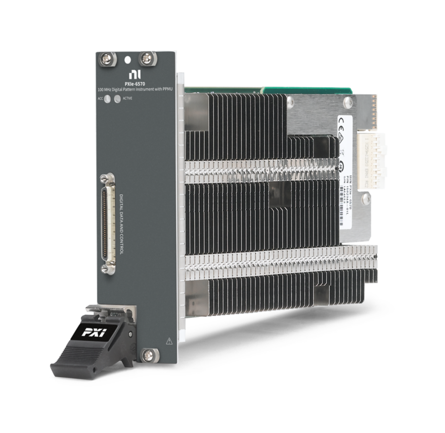
2槽,100 MVector/s PXI数字pattern仪器
ONETEST 欢迎您
厂商登录 | 入驻
登录 | 注册 购物车 微信公众号厂商登录
最大有源负载:24 mA
模块宽度:2
双向数字通道数量:32
可支持的硬件平台:PXI
2槽,100 MVector/s PXI数字pattern仪器
以下指标取自 Teledyne 官方在线规格书,按原文档小节分组。
| 375726J-01 | November 2026 |
| 375726H-01 | September 2026 |
| 375726G-01 | July 2025 |
| 375726F-01 | April 2025 |
| 375726E-01 | June 2018 |
| 375726D-01 | June 2017 |
| 375726C-01 | May 2017 |
| 375726B-01 | October 2016 |
| Data | DIO <0..31> |
| Ground | GND |
| Ground | DGS |
| Analog | CAL MEASURE |
| Analog | CAL SENSE |
| Analog | CAL GND |
| Analog | CAL FORCE |
| N/A | RESERVED |
| Channel count | 32 |
| NI-Digital Pattern Driver 16.0 | 4 |
| NI-Digital Pattern Driver 17.0 and later | 8 |
| System channel count[1] | 256 |
| Large Vector Memory (LVM) | 128M vectors |
| NI-Digital Pattern Driver 17.5 and earlier | 1,023 cycles |
| NI-Digital Pattern Driver 18.0 and later | (8,192/N sites)-1 cycles |
| Maximum allowable offset (DGS minus GND) | ±300 mV |
| Supported measurement range[2] | -2 V to 7 V[3] |
| Maximum vector rate | 100 MHz |
| Vector period range | 10 ns to 40 µs (100 MHz to 25 kHz) |
| Vector period resolution | 38 fs |
| Vector period | Vector-by-vector on the fly |
| Edge timing | Per channel, vector-by-vector on the fly |
| Drive formats | Per channel, vector-by-vector on the fly |
| Master clock source | PXIe_CLK100[4] |
| Sequencer clock domains | One (independent sequencer clock domains on a single instrument not supported) |
| 100 MHz maximum vector rate | Non-Return (NR), Return to Low (RL), Return to High (RH) |
| 50 MHz maximum vector rate | Surround by Complement (SBC)[5] |
| Compare formats | Edge strobe |
| NI-Digital Pattern Driver 17.5 and earlier | 1x |
| NI-Digital Pattern Driver 18.0 and later | 1x, 2x |
| NI-Digital Pattern Driver 17.5 and earlier | 4; drive on, drive data, drive return |
| NI-Digital Pattern Driver 18.0 and later | 6; drive on, drive data, drive return, drive data 2, drive return 2, drive off |
| NI-Digital Pattern Driver 17.5 and earlier | 1; strobe |
| NI-Digital Pattern Driver 18.0 and later | 2; strobe, strobe 2 |
| Number of time sets[6] | 31 |
| Minimum | Start of vector period (0 ns) |
| Maximum | 5 vector periods or 40 µs, whichever is smaller |
| Between any driven data change (NI-Digital Pattern Driver 17.5 and earlier) | 5 ns |
| Between any driven data change (NI-Digital Pattern Driver 18.0 and later) | 3.75 ns |
| Between any Drive On and Drive Off edges | 5 ns |
| Between Compare Strobes | 5 ns |
| Edge placement resolution | 39.0625 ps |
| TDR deskew adjustment resolution | 39.0625 ps |
| Edge Multiplier = 1x | ±500 ps, warranted |
| Edge Multiplier = 1x | ±500 ps, warranted |
| Edge Multiplier = 2x | Bit rate ≤ 200 Mbps: ±500 ps, typical |
| Edge Multiplier = 2x | Bit rate ≤ 266 Mbps: ±600 ps, typical |
| Edge Multiplier = 1x | ±500 ps, warranted |
| Edge Multiplier = 1x | ±500 ps, warranted |
| Edge Multiplier = 2x | Bit rate ≤ 100 Mbps: ±500 ps, typical |
| Edge Multiplier = 2x | Bit rate ≤ 133 Mbps: ±700 ps, typical |
| Edge Multiplier = 1x | ±1.5 ns, warranted |
| Edge Multiplier = 1x | ±1.5 ns, warranted |
| Edge Multiplier = 2x | Bit rate ≤ 200 Mbps: ±1.5 ns, typical |
| Edge Multiplier = 2x | Bit rate ≤ 266 Mbps: ±1.8 ns, typical |
| Signal type | Single-ended, referenced to the DGS pin when connected. Otherwise referenced to GND. |
| Programmable levels | VIH, VIL, VTERM |
| Range (VIH, VIL, VTERM) | -2 V to 6 V |
| Minimum swing (VIH minus VIL) | 400 mV, into a 1 MΩ load |
| Resolution (VIH, VIL, VTERM) | 122 µV |
| Accuracy (VIH, VIL, VTERM) | ±15 mV, 1 MΩ load, warranted |
| Maximum DC drive current | ±32 mA |
| Output impedance | 50 Ω |
| Rise/fall time, 20% to 80% | 1.2 ns, up to 5 V |
| Signal type | Single-ended, referenced to the DGS pin when connected. Otherwise referenced to GND. |
| Programmable levels | VOH, VOL |
| Range (VOH, VOL) | -2 V to 6 V |
| Resolution (VOH, VOL) | 122 µV |
| Accuracy (VOH, VOL) | ±25 mV, from -1.5 V to 5.8 V, warranted |
| Programmable input termination modes | High Z, 50 Ω to VTERM, Active Load |
| Leakage current | <15 nA, in the High Z termination mode |
| Programmable levels | IOH, IOL |
| Range | -2 V to 6 V |
| Resolution | 122 µV |
| Range | 150 µA to 24 mA |
| Resolution | 488 nA |
| Accuracy | ±14 µA for current level ≤512 µA, typical ±93 µA for current level >512 µA, typical |
| Signal type | Single-ended, referenced to the DGS pin when connected. Otherwise referenced to GND. |
| Range (NI-Digital Pattern Driver 17.5 and earlier) | -2 V to 6 V |
| Range (NI-Digital Pattern Driver 18.0 and later) | -2 V to 6 V 6 V to 7 V in Extended Voltage Range |
| Resolution | 122 μV |
| Accuracy (NI-Digital Pattern Driver 17.5 and earlier) | ±15 mV, 1 MΩ load, from -2 V to 6 V, warranted |
| Accuracy (NI-Digital Pattern Driver 18.0 and later) | ±15 mV, 1 MΩ load, from -2 V to 6 V, warranted ±50 mV, 1 MΩ load, from 6 V to 7 V, typical |
| Signal type | Single-ended, referenced to the DGS pin when connected. Otherwise referenced to GND. |
| Range | -2 V to 6 V |
| Resolution | 228 μV |
| Accuracy | ±5 mV, warranted |
| ±2 µA | 60 pA |
| ±32 µA | 980 pA |
| ±128 μA | 3.9 nA |
| ±2 mA | 60 nA |
| ±32 mA | 980 nA |
| Range | -2 V to 6 V |
| Resolution | 122 μV |
| Accuracy | ±100 mV, typical |
| ±2 μA | 460 pA |
| ±32 μA | 7.3 nA |
| ±128 μA | 30 nA |
| ±2 mA | 460 nA |
| ±32 mA | 7.3 μA |
| Minimum | 4 μs |
| Maximum | 65 ms |
| Resolution | 4 μs |
| Flow Control | repeat jump jump_if set_loop end_loop exit_loop exit_loop_if call return keep_alive match halt scan |
| Sequencer Flags and Registers | set_seqflag clear_seqflag write_reg |
| Signal and Trigger | set_signal pulse_signal clear_signal reset_trigger |
| Digital Source and Capture | capture_start capture capture_stop source_start source source_d_replace |
| Minimum delay between source_start opcode and the first source opcode or subsequent source_start opcode | 3 μs |
| Matched and failed condition pipeline latency | 80 cycles |
| Operation modes | Serial and parallel; broadcast and site-unique |
| Source memory size | 32 MB (256 Mbit) total |
| Maximum waveforms | 512 |
| Operation modes | Serial and parallel; site-unique |
| Capture memory size | 1 million samples |
| Maximum waveforms | 512 |
| Number of clock generators | 32 (one per pin) |
| Clock period range | 6.25 ns to 40 μs (160 MHz to 25 kHz)[7] |
| Clock period resolution | 38 fs |
| Range | 5 kHz to 200 MHz, 2.5 ns minimum pulse width |
| Accuracy | See Calculating Frequency Counter Error |
| 1 | 220 |
| 10 | 70 |
| 100 | 22 |
| 1000 | 7 |
| Time Measurement Units per module | 2 |
| Measurements | Rise or fall time Period Frequency (derived from period measurements) Pulse widths Duty cycles Channel-to-channel skew (delay between channels) Custom measurements based on selecting start and stop events and polarities |
| Voltage thresholds and other comparator specifications | Refer to the Comparator section. |
| Timing resolution | 167 ps |
| Input conditioning | Configurable debounce time, up to 1.275 μs |
| Sample averaging | No averaging (single shot) up to 4,294,967,295 samples per averaged result. |
| Arm type | Edge or Immediate |
| Measurable delay range | ±10.7 s |
| Minimum signal period for a period measurement | 25 ns |
| Minimum rearm time after a sample (non-period measurement) | 35 ns |
| Minimum measurable delay magnitude when arm type is Edge (non-period measurement) | Typically 2 ns |
| Minimum measurable delay when arm type is Immediate (non-period measurement) | No minimum |
| Systematic error in period measurements (typical input frequencies) | ±100 ps |
| Systematic error in period measurements (input frequencies correlated with 6 GHz) | ±200 ps |
| Systematic error in single-channel measurements other than period | ±500 ps |
| Systematic error in channel skew measurements (channel-to-channel delay measurements) | ±750 ps |
| Input power | 68 W |
| 3.3 V | 4.4 A |
| 12 V | 4.7 A |
| Operating | 0 °C to 45 °C |
| Storage | -40 °C to 71 °C |
| Operating | 10% to 90%, noncondensing |
| Storage | 5% to 95%, noncondensing |
| Pollution degree | 2 |
| Maximum altitude | 2,000 m (800 mbar) (at 25 °C ambient temperature) |
| Operating vibration | 5 Hz to 500 Hz, 0.3 g RMS |
| Non-operating vibration | 5 Hz to 500 Hz, 2.4 g RMS |
| Operating shock | 30 g, half-sine, 11 ms pulse |
| Module type | 3U, two-slot, PXI Express module |
| Dimensions | 131 mm × 42 mm × 214 mm (5.16 in. × 1.65 in. × 8.43 in.) For more information, visit ni.com/dimensions and search by module number. |
| Weight | 920 g (32.45 oz.) |
官方规格书:https://www.ni.com/docs/en-US/bundle/pxie-6570-specs/page/specs.html
NI官方渠道
官方渠道(官网 / 热线 / 邮箱)
官方渠道(中国大陆)
• 官网 www.ni.com/zh-cn
• 在线选购 www.ni.com/zh-cn/shop.html
• 经销商查询
官网「查找经销商」 www.ni.com/zh-cn/shop/advisors.html
• 联系方式
NI 中文官网不公布中国区电话与邮箱,报价、技术支持、校准、维修一律通过官网在线表单提交(「联系我们」页)
全国办事处
公司总部
• NI(National Instruments)
• 地址
11500 N Mopac Expwy, Austin, TX 78759-3504, United States
• 母公司
Emerson(2023 年完成收购,NI 隶属艾默生测试与测量业务集团)
0条提问
X
提问
X
回答
发表口碑

AI问答




 粤公网安备44030902003758