


 客服
客服




该型号官方中文站未提供独立中文产品手册,本节内容依据官方产品页与官方规格书整理。
ONETEST 欢迎您
厂商登录 | 入驻
登录 | 注册 购物车 微信公众号厂商登录
类似产品
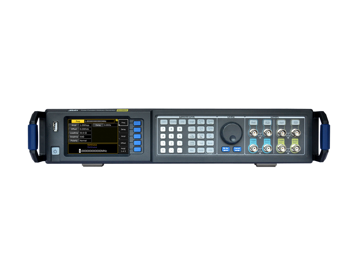
● 具有两个特性相同的独立输出通道● 每通道具有Out和Out非输出,可组合成单端和差分输出● 具有脉冲波、正弦波、方波、斜波、噪声、码型和任意波形● 具有FM、AM、PM、PWM、FSK、Sweep、Burst模式● 脉冲波边沿时间最小2.5 ns,上升、下降可独立调整● 脉冲波最大频率120 MHz,正弦波最大频率240 MHz● 信号幅度最大10 Vrms(负载50 Ω),直流偏置最大10 Vdc(负载50 Ω)
● 14 bit、2 GSa/s、每通道512K采样深度的任意波形● 可产生高达120 Mbit/s的理想和任意比特形状码型● 配置U盘存储器接口、USB设备接口,LAN接口、GPIB接口。
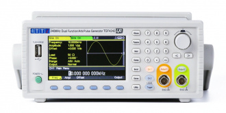
正弦波频率范围:TGF4242为0.001mHz至240MHz,TGF4162为160MHz,TGF4082为80MHz,TGF4042为40MHz。高纯度正弦波,具有低相位噪声和抖动,音频带THD低至0.05%。可变占空比的方波高达100MHz,边沿速度低至3ns。分辨率高达15位或1µHz,高稳定性TCXO时间基准。两个相同的通道 - 独立或通过耦合和跟踪模式连接。通道间相位偏移为-3600至+3600,分辨率为0.0010。1mHz至100MHz的脉冲生成,具有100ps宽度分辨率,<30ps抖动,并且上升/下降时间可独立变化。高达100MHz噪声带宽的宽带噪声发生器。具有8种序列长度的PRBS伪随机二进制序列生成*。使用高达16个谐波的谐波发生器*。内置广泛的标准和任意波形。任意波形为14位/400MSa/s(TGF4042 & TGF4082)或16位/800MSa/s(TGF4162 & TGF4242)。包含Windows版波形管理软件Waveform Manager Plus,用于编辑。前置USB主机插座,用于通过闪存驱动器进行波形存储和文件传输。包括Sum*调制在内的全面的内部/外部数字和模拟调制套件。调制频率高达内部10MHz和外部5MHz。带内部和外部触发的门控和突发模式。使用内部或外部触发进行双向线性和对数扫描。具有五种测量模式的125MHz频率计数器/定时器。可通过USB和LAN(LXI)接口编程;GPIB为可选
l 波形重复次数1-65535次或连续l 输出频率范围正弦波:10mHz~15MHz方波:10mHz~15MHz脉冲:10mHz~5MHz三角波、斜波:10mHz~100kHzl 波形存贮器长度:128kSa/CHl 输出阻抗:50Ωl 输出幅度:10mVpp~10Vppl 输出精度:±1%±10mVpp(频率在1kHz时)l 波形输出触发方式:软件触发、外触发、PXI触发l 外触发信号:边沿触发,TTL电平
同厂商产品
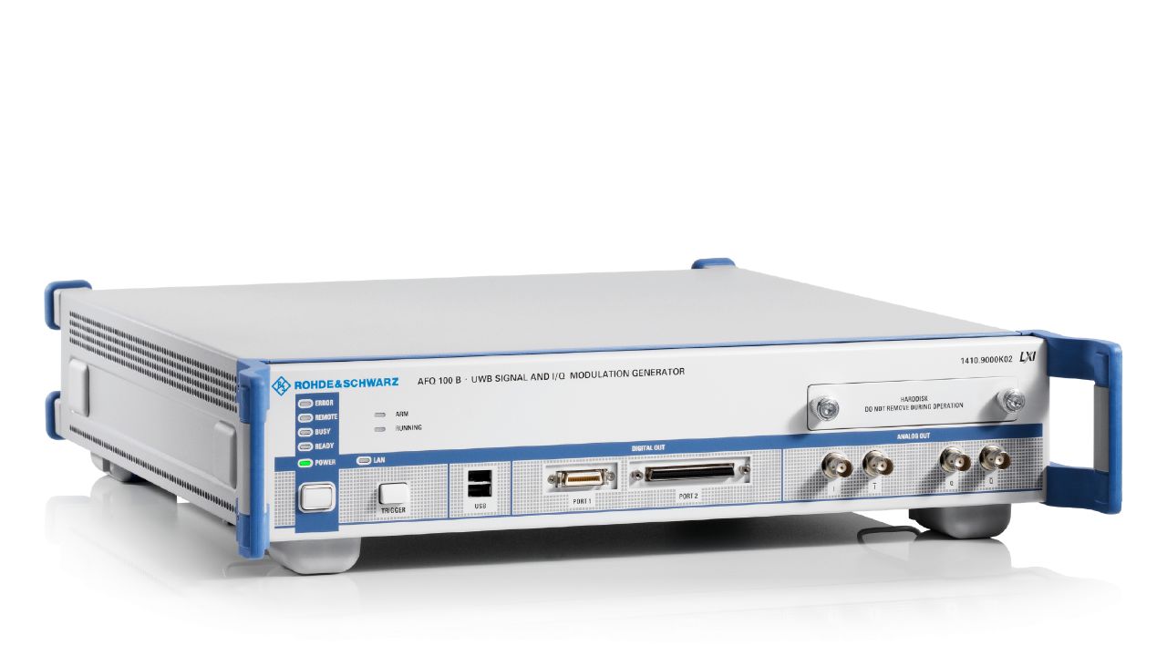
超宽带信号和I/Q调制发生器适用于需要高带宽的应用,例如支持超宽带信号等宽带数字通信系统或航空航天和国防雷达应用。
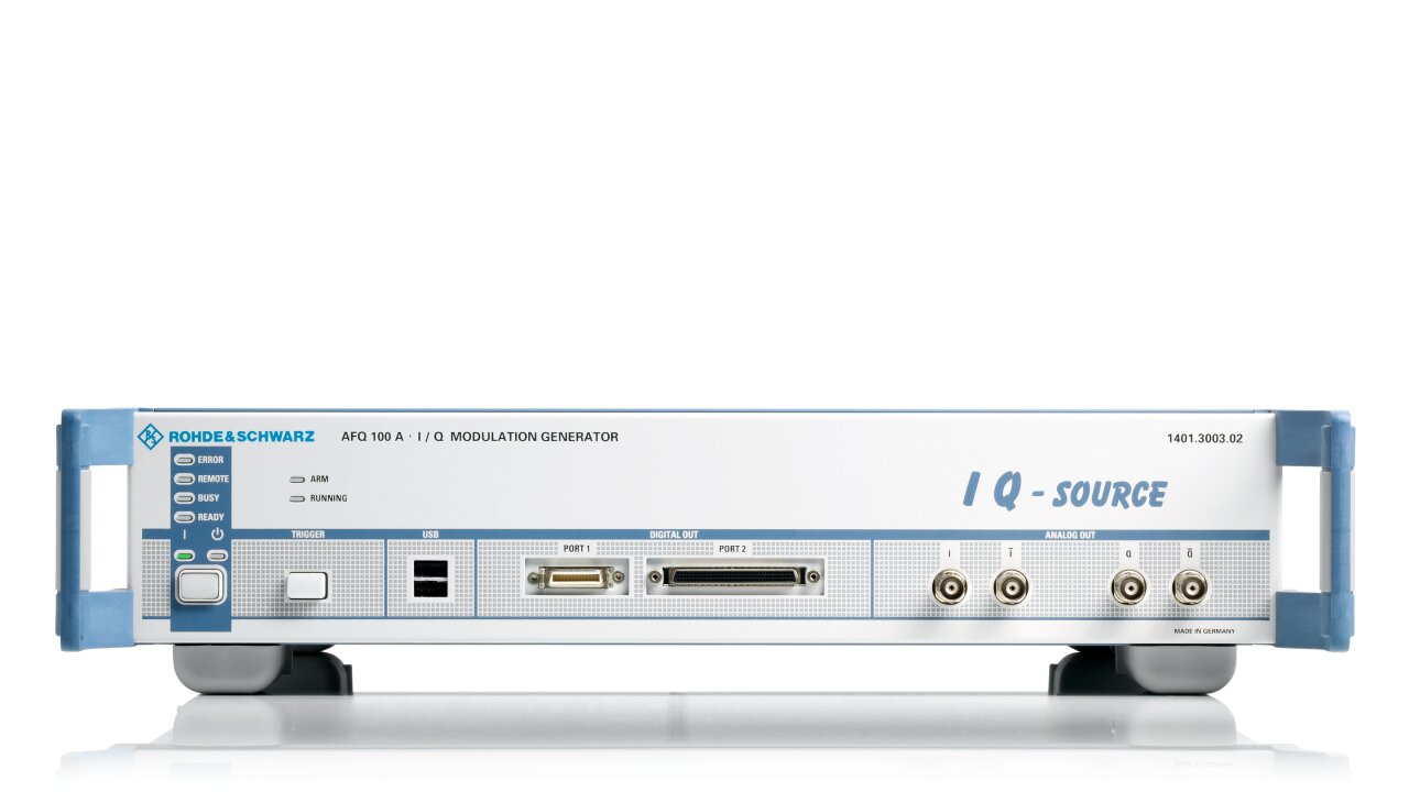
AFQ100A 1kHz至300MHzI/Q 调制发生器|罗德与施瓦茨 (在产)
产品描述
详细指标
软件和手册|白皮书
购买渠道
选件
问大家
视频
测评
口碑
系统与解决方案
罗德与施瓦茨 · Rohde & Schwarz
AFQ100A I/Q 调制发生器
R&S®AFQ100A 是罗德与施瓦茨的 I/Q 调制发生器。官方目录位于「信号发生器 / 基带信号发生器」。官方标称频率:1 kHz至300MHz。官方技术指标共 63 组、190 项,详见「详细指标」。
产品简介
该型号官方中文站未提供独立中文产品手册,本节内容依据官方产品页与官方规格书整理。
官方公布的主要指标:频率 1 kHz至300MHz;分辨率 1 × 10⁻⁷;输入阻抗 50 Ω/1 kΩ, switchable;Memory clock of the R&S®AFQ100A 1 kHz至300MHz;Memory clock of the R&S®AFQ100B 1 kHz至300MHz (mode 1), 600MHz (mode 2)。
官方公布的产品型号:AFQ100A、AFQ100B。
核心参数
• 频率:1 kHz至300MHz
• 分辨率:1 × 10⁻⁷
• 输入阻抗:50 Ω/1 kΩ, switchable
• Memory clock of the R&S®AFQ100A:1 kHz至300MHz
• Memory clock of the R&S®AFQ100B:1 kHz至300MHz (mode 1), 600MHz (mode 2)
• waveform memory (R&S®AFQ-B:up至1 Gsample
• the R&S®AFQ100B:(mode 1),
• Waveform bandwidth:max. 0.33 × memory clock 1,
产品型号
• 官方型号:AFQ100A、AFQ100B
资源下载
详细指标请见 AFQ100A 详细指标页。
罗德与施瓦茨 Rohde & Schwarz · onetest 仪器资源库
以下为 R&S®AFQ100A 的官方技术指标,共 63 个指标组、190 项。
参数名以行业通用中文术语为主(其中 158 项保留官方规格书原文),数值与单位保留官方规格书原样。
技术指标
• AFQ100A_AFQ100B_dat_sw_en_5214-0799-22_v0400_Cover.indd:1 | 10.02.2017 | 09:52:51
Output memory
• Memory clock of the R&S®AFQ100A:1 kHz至300MHz
• Memory clock of the R&S®AFQ100B:1 kHz至300MHz (mode 1), 600MHz (mode 2)
• waveform memory (R&S®AFQ-B:up至1 Gsample
• the R&S®AFQ100B:(mode 1),
(mode 2)
• waveform memory (R&S®AFQ-B:up至1 Gsample
• waveform memory (R&S®AFQ-B:up至512 Msample
• Waveform bandwidth:max. 0.33 × memory clock 1,
max. 0.44 × memory clock 2
• Marker channels:4
Clock generation
• 600MHz
• converter clock (with digital lowpass filter:1200MHz
and clock rate converter)
• data clock:700MHz (in line with TIA644)
• memory clock:1kHz to interface clock rate
response correction
• with data enable:valid samples are marked with a "data
clock
• (LVDS, parallel):data clock same as interface clock
(direct output, no filters)
• memory clock:same as interface clock
• 分辨率:1 × 10⁻⁷
• Clock output:memory clock
• level:LVTTL, 2 V into 50 Ω
• 10 mV and 1.9 V
• 输入阻抗:50 Ω/1 kΩ, switchable
• 频率:1 kHz至300MHz
Reference frequency
• Output for internal reference:frequency | 10MHz
• aging (after 30 days of operation):1 × 10⁻⁶/year
• temperature effect (+5 °C to +45 °C):1 × 10⁻⁶
• level:0.35 V (rms, sinewave, into 50 Ω)
• output impedance:50 Ω
• Input for external reference:frequency | 10MHz
• permissible frequency deviation:0.05 %
• level:0.2 V至2 V (rms, sinewave)
• 输入阻抗:50 Ω
Signal output
• Number of outputs:2 (I and Q)
• Output (unbalanced) of the:1 V (Vpp) (into 50 Ω (nominal))
• AFQ100A:level range | 0 V至1.5 V (Vpp) (into 50 Ω)
• hardware attenuator:0 dB至21 dB in steps of 3 dB
• fine variation:±5 %, separately for I and Q channel
• 分辨率:14 bit
• 阻抗:50 Ω each
• pulse rise/fall time (10 %/90 %):6 ns
• level error (DC, at 1 V (Vpp)):< ±1 % (at 1kHz, after auto alignment)
• frequency response (relative to DC):±0.05 dB up至50MHz ±0.1 dB up至100MHz
• AFQ100B:should be terminated with 50 Ω
• Output (balanced) of the R&S®AFQ100A:2 V (Vpp)
(between I and Ī into 100 Ω, nominal)
• level range:0 V至3 V (Vpp) (into 100 Ω)
• hardware attenuator:0 dB至21 dB in steps of 3 dB
• fine variation:±5 %, separately for I and Q channel
• 分辨率:14 bit
• 阻抗:50 Ω each
• bias voltage:2.5 V to +2.5 V in steps of 10 mV
• pulse rise/fall time (10 %/90 %):6 ns
• level error (DC, at 2 V (Vpp)):< ±1 % (at 1kHz, after auto alignment)
bias voltage OFF)
• < ±0.5 % (at 1kHz, after auto alignment,
bias voltage ON)
• frequency response (relative to DC):±0.05 dB up至50MHz ±0.1 dB up至100MHz
nominal)
• level range:0 V至1.4 V (Vpp) (into 100 Ω)
• hardware attenuator:0 dB, 6 dB
• fine variation:±5 %, separately for I and Q channel
• 分辨率:14 bit
• 阻抗:50 Ω each
• bias voltage:2.5 V to +2.5 V in steps of 10 mV
• pulse rise/fall time (10 %/90 %):2.5 ns
• level error (DC, at 1 V (Vpp)):< ±1 % (at 1kHz, after auto alignment)
bias voltage OFF)
• < ±0.5 % (at 1kHz, after auto alignment,
bias voltage ON)
• typ. 0.3 dB
mode 2: ±0.8 dB up to 100 MHz,
• typ. 0.5 dB
• ±1 dB up至150MHz
• ±2 dB up至240MHz
• ±2.5 dB up至264MHz
harmonics
• 10 MHz signal:< -70 dBc, typ. -75 dBc
Vout = 1 V (Vpp), bias voltage OFF)
• 50 MHz signal:< -65 dBc, typ. -68 dBc
Vout = 1 V (Vpp), bias voltage OFF)
• 100 MHz signal:typ. -50 dBc
Vout = 1 V (Vpp), bias voltage OFF)
• 3GPP signal, test model 1/64
(Vout = 1.5 V (Vpp), bias voltage OFF) 3
• adjacent channel:typ. -80 dBc
• alternate channel:typ. -80 dBc 3GPP signal, test model 1/64
f(IF) = 25 MHz)
• adjacent channel:typ. -75 dBc
• alternate channel:typ. -77 dBc
harmonics
• 1 MHz signal,:< -70 dBc, typ. -75 dBc
Vout = 0.5 V (Vpp)
• 10 MHz signal,:< -70 dBc, typ. -75 dBc
Vout = 0.5 V (Vpp)
• 50 MHz signal,:< -55 dBc, typ. -60 dBc
Vout = 0.5 V (Vpp)
• 100 MHz signal,:typ. -55 dBc
Vout = 0.5 V (Vpp)
• 150 MHz signal,:typ. -50 dBc
Vout = 0.5 V (Vpp)
• Noise floor:at Vpp = 0.7 V | < -154 dBc (1Hz)
• Digital filters:4 filters (15 taps each) in butterfly
structure 4
• Skew between I and Q channel:2 ns to +2 ns
(can be digitally set in steps of 10 ps) 4
• residual offset:< ±1 mV (after auto alignment)
存储器
• Single output:single output of waveform from output
存储器
• Segment mode:output of up至2048 different segments;
can be selected
• Trigger inputs:2, TRIG and NEXT (BNC)
• input level:0 V至3 V, threshold can be set between 10 mV and 1.9 V
• 输入阻抗:50 Ω/1 kΩ, switchable
• pulse width:min. 10 ns
• min. trigger repetition period:100 μs + 25 memory clock cycles
synchronized with the trigger input
• Direct IF:digital modulator for direct generation of
Auxiliary outputs
• Markers:user-configurable signals aligned to data
words
• number:4, BNC
• level:LVTTL, 2 V into 50 Ω
BERT (R&S®AFQ-K80 option)
• Pseudo-random binary sequences:PRBS9, PRBS11, PRBS15, PRBS16,
PRBS20, PRBS21, PRBS23
• Clock source:clock signal supplied by DUT; one clock
pulse is required for each valid bit
• Clock rate:min. 1kHz, max. 100MHz
• 接口:BNC
• data:TTL
• clock:TTL
• setup time:4 ns
• hold time:0 ns
• Polarity:normal and inverted (data, clock)
• input level:0 V至3 V, selectable threshold
• 输入阻抗:50 Ω/1 kΩ, switchable
• Results:BER in ppm
Digital outputs (R&S®AFQ-B18 option)
• Output:port 1 multiplexed I/Q data stream, compatible
with other Rohde & Schwarz equipment
• port 2:parallel I/Q interface
• Port 1:operating modes
interface clock)
• with enable:valid samples are marked with a "data
valid" bit in the data stream
• clock source:external, internal
• 接口:26-pin I/Q interface
• data:LVDS
• clock:LVDS
• Port 2:operating mode direct output of memory data
• clock source:external, internal
• 接口:68-pin HD-SCSI, 16 bit for each I and Q, 2 data clock lines
• data:LVDS, >±200 mV into 100 Ω
• clock:LVDS, >±200 mV into 100 Ω
• skew:200 ps
• 上升时间:400 ps
一般数据
• Computer:industrial PC
• Mass memory:3.5" SATA hard disk drive, 160 Gbyte
• 接口:USB 2.0 (master and slave), Gigabit
Ethernet, IEC 625 (IEEE 488)
• Operating software updates:via USB
• 远程控制:via USB, Ethernet, IEC 625-2 (IEEE 488)
• Command set:SCPI 1996.0 with extensions
• IEC/IEEE interface functions:SH1, AH1, T6, L4, SR1, RL1, PP1, DC1,
Operating data
• 电源:100 V至240 V AC, 50 Hz至60Hz, 2.0 A至1.0 A
• power factor correction:in line with EN 61000-3-2
• EMC:in line with EN 55011 class B, EN 61326
EN 61326
• immunity to RFI:10 V/m
in line with IEC 68-2-1 and IEC 68-2-2
• storage temperature range:40 °C to +70 °C
climatic stress
• damp heat:95 % relative humidity at +40 °C;
in line with EN 60068-2-6
• vibration, random:10 Hz至300Hz, acceleration 1.2 g (rms)
in line with EN 60068-2-64
• shock:40 g shock spectrum,
in line with EN 60068-2-27, MIL-STD-810E
• Electrical safety:in line with IEC 1010-1, EN 61010-1,
UL 61010-1, CAN/CSA-C22.2
• No. 61010-1-04
• Approvals:VDE-GS, CCSAUS
• 尺寸:W × H × D | 426.7 mm × 87.6 mm × 450 mm
(16.80 in × 3.45 in × 17.72 in)
• 重量:when fully equipped | 7.5 kg
(16.53 lb)
• Recommended calibration interval:3 years
订购信息
• Designation:Type Order No.
• I/Q Modulation Generator 5:AFQ100A | 1401.3003.02
• UWB Signal and I/Q Modulation Generator 6:AFQ100B | 1410.9000.02
Baseband hardware
• Waveform Memory 256 Msample 7:AFQ-B10 | 1401.5106.02
• Waveform Memory 1 Gsample:AFQ-B11 | 1401.5206.02
• Waveform Memory 512 Msample 8:AFQ-B12 | 1411.0007.02
• Digital I/Q Output:AFQ-B18 | 1401.5306.02
Baseband software
• Bit Error Ratio Tester:AFQ-K80 | 1401.5006.02
Digital standards using R&S®WinIQSIM2™ PC software
• GSM/EDGE:AFQ-K240 | 1401.6302.02
• EDGE Evolution:AFQ-K241 | 1401.6102.02
• 3GPP FDD:AFQ-K242 | 1401.6354.02
• 3GPP FDD Enhanced MS/BS Tests, incl. HSDPA:AFQ-K243 | 1401.6402.02
• GPS 1 Satellite:AFQ-K244 | 1401.6454.02
• HSUPA:AFQ-K245 | 1401.6504.02
• CDMA2000® incl. 1xEV-DV:AFQ-K246 | 1401.6554.02
• 1xEV-DO Rev. A:AFQ-K247 | 1401.5958.02
• IEEE 802.11 (a/b/g):AFQ-K248 | 1401.6602.02
• IEEE 802.16:AFQ-K249 | 1401.6654.02
以上为前 161 项指标;完整指标(共 190 项)见官方规格书(本页底部「资源下载」)。
型号与选件
• 官方型号:AFQ100A、AFQ100B
指标整理自官方文件:AFQ100A_AFQ100B_dat_sw_en_5214-0799-22_v0400.pdf
资源下载
罗德与施瓦茨 Rohde & Schwarz · onetest 仪器资源库