是德科技 | KEYSIGHT
AP5002A 9kHz至26GHz 信号发生器 +23dBm 详细指标
Analog Signal Generators
条件:Nominal (Unless otherwise indicated) Note
Frequency range
9 kHz to 12 GHz AP5002A-512
9 kHz to 20 GHz AP5002A-520
9 kHz to 26 GHz AP5002A-526
Frequency / Amplitude settling time
200 μs
30 μs Options UNZ, UNQ
≤20 ms Only when crossing option
1E1
power ranges including manual
1E1
selection via SCPI command
1
Internal reference frequency
100 MHz
Initial accuracy of internal reference ± 40 ppb calibrated at 23
± 3 °C at the time of
calibration, user adjustable
Temperature stability (0 to 45 °C)
±100 ppb
Aging per day (after
30 days of
Internal reference output range 10 MHz, 100 MHz Both
10 MHz and 100 MHz reference
输出 available 开 REF OUT 端口
条件:lower than -20 dBm , as long as 1E1 power ranges are not being crossed during the signal change.
Internal reference output power
0 dBm
1 With manual
1E1 selection, the user can move the fast dynamic range (30 μs settling time with UNZ/UNQ) to a power range
Internal reference output impedance
50 Ω
Bypass internal reference input 100 MHz
-5 to +10 dBm High phase synchronous mode
Phase lock to ext. ref. input range
1 MHz to 250 MHz User programmable
Reference input level
-5 to +13 dBm
Reference input impedance
50 Ω
条件:With Option 1E1 -120 dBm +12 dBm 9 to < 100 kHz
With Option 1EA -20 dBm +12 dBm 9 kHz to < 100 kHz
(typical) in range 0 to 45 °C). Nominal unless otherwise indicated.
2 Not warranted below -20 dBm (standard) / below -70 dBm (with Option 1E1)
Figure 1. Nominal maximum output power, 9 kHz to 1 MHz, with Option 1EA
Figure 2. Nominal maximum output power, 100 kHz to 26 GHz, with Option 1EA
Figure 3. Nominal frequency response, 0 to 20 GHz, at -20, 0, and +20 dBm
Figure 4. Nominal absolute power level error, 0 to 20 GHz, at -20, 0, and +20 dBm
Standard -20 dBm +12 dBm 9 to <
100 kHz
-20 dBm +15 dBm
100 kHz to 25 GHz
-20 dBm +10 dBm >
25 to 26 GHz
-120 dBm +15 dBm
100 kHz to 25 GHz
-120 dBm +10 dBm >
25 to 26 GHz
-20 dBm +20 dBm 100 kHz to <
50 MHz
-20 dBm +23 dBm
50 MHz to 7.5 GHz
-20 dBm +20 dBm >
7.5 to 18 GHz
-20 dBm +18 dBm >
18 to 20 GHz
-20 dBm +16 dBm >
20 to 25 GHz
-20 dBm +10 dBm >
25 to 26 GHz
and 1EA
-120 dBm +12 dBm 9 to <
100 kHz
-120 dBm +20 dBm 100 kHz to <
50 MHz
-120 dBm +23 dBm
50 MHz to 7.5 GHz
-120 dBm +20 dBm >
7.5 to 18 GHz
-120 dBm +18 dBm >
18 to 20 GHz
-120 dBm +16 dBm >
20 to 25 GHz
-120 dBm +10 dBm >
25 to 26 GHz
(ALC mode on, flatness correction: up to 2,000 points, temperature effects
0.015 dB/ °C
Power range > +15 dBm to Pmax -15 to +15 dBm -70 to < -15 dBm <
-70 to -120 dBm
9 kHz to 10 GHz
±1.6 dB (spec)
±0.8 dB
±1.0 dB (spec),
±0.3 dB
±1.5 dB (spec),
±0.4 dB
±1.8 dB
10 GHz to fmax
±1.6 dB (spec)
±0.8 dB
±1.0 dB (spec),
±0.3 dB
±1.5 dB (spec),
±0.4 dB
±2.0 dB
VSWR 1.5 ≤ 6 GHz 2.0 >
6 GHz
条件:Figure 5. Nominal phase noise at different frequencies, 1 Hz to 100 MHz offset
SSB Phase Noise 1 GHz, 20 kHz offset -130 dBc/Hz 4 GHz, 20 kHz offset -118 dBc/Hz 20 GHz, 20 kHz offset
-104 dBc/Hz
Wideband noise -150 dBc/Hz at 5 GHz, +15 dBm
+15 MHz offset
Amplitude noise at 10 GHz
-130 dBc/Hz
Output harmonics -40 dBc -30 dBc Pout = +5 dBm
2nd and 3rd harmonics tested to 26 GHz
Sub-harmonics -75 dBc Fcarrier ≤
20 GHz
-50 dBc Fcarrier >
20 GHz
条件:Figure 6. Nominal harmonics, Pout = +5 dBm
≤ 312 MHz -80 dBc CW, Pout = +10 dBm, >
3 kHz offset
> 312 to 625 MHz -75 dBc CW, Pout = +10 dBm, >
3 kHz offset
> 625 MHz to 1.5 GHz -75 dBc CW, Pout = +10 dBm, >
3 kHz offset
> 1.5 to 2.5 GHz -70 dBc CW, Pout = +10 dBm, >
3 kHz offset
> 2.5 to 5 GHz -65 dBc CW, Pout = +10 dBm, >
3 kHz offset
> 5 to 10 GHz -60 dBc CW, Pout = +10 dBm, >
3 kHz offset
> 10 to 20 GHz -55 dBc CW, Pout = +10 dBm, >
3 kHz offset
> 20 GHz -50 dBc CW, Pout = +10 dBm, >
3 kHz offset
Residual FM at 10 GHz 15 Hz
0.3 kHz to 3 kHz, weighted, (ITU-T), RMS
Residual AM at 10 GHz
0.02% RMS value (0.01 kHz to 15 kHz)
Digital Power / Frequency / List Sweep (Sweep Type: Linear, Logarithmic, Random)
Switching Speed (tswitch)
3
tswitch = tdelay + tsettling
400 μs to 19998 s standard
≤ 40 μs (spec)
4 Option UNZ
≤ 40 µs 3 fstep <
2.2 GHz, Option UNQ
100 µs 3 fstep ≥
2.2 GHz, Option UNQ
≤20 ms Only when crossing option
1E1 power
ranges including manual
1E1 selection
Setup time (tsetup) ≥
10 μs Time required, after settling, for unit to
be ready to accept another trigger
On-time (dwell time) range
0 to 21 s Pulse on time in pulsed sweep or list
Off-time range (incl. settling time)
0 to 21 s Pulse off time in pulsed sweep or list
Settling time (tsettling)
270 µs
30 µs Options UNZ, UNQ
Timing delay (tdelay)
2 to 10 µs Trigger input to start of transition
100 ns Trigger input to start of transition,
条件:3 Frequency switching speed is defined as the time it takes, after receipt of trigger, to change frequency or amplitude and
settle to 1000 ppm of its final value or within 1000 Hz, whichever is greater. Amplitude Switching speed is defined as the
time it takes, after receipt of trigger, to change and settle to 0.5 dB of its final value.
typical for all other ALC modes and across the power ranges supported by fixed attenuation settings.
lower than -20 dBm, as long as 1E1 power ranges are not being crossed during the signal change.
5 ns Options UNZ, UNQ
Timing accuracy per point
3 μs
5 ns Options UNZ, UNQ
Sweep list length
2 to 10000
4 Fast switching speed specifications are tested and guaranteed only for −40 dBm to +10 dBm, step size ≤
15 dB, high to
low sweep not below
-20 dBm and only applicable with manual attenuation and ALC enabled. Switching performance is
5 With manual 1E1 selection, the user can move the fast dynamic range (
30 μs settling time with UNZ/UNQ) to a power range
All modulation types (FM, PM, AM, and pulse modulation) may be enabled simultaneously except that
FM and phase modulation cannot be combined. For example, AM and FM can run concurrently and
On/off ratio
75 dB at +10 dBm
Repetition frequency range DC to 10 MHz
Pulse width range
100 ns to 5 s ALC mode hold (ALC locked allowing
for faster modulations that would otherwise exceed ALC bandwidth)
30.281 ns to 5 s ALC mode hold (ALC locked allowing for faster modulations that would
otherwise exceed ALC bandwidth),
Option UNQ, UNZ
500 ns ALC mode on
Pulse rise/fall time 30 ns <
5 GHz
Duty cycle range
0.05% to 99.95%
Pulse resolution
30.281 ns
5 ns Options UNQ, UNZ
External input threshold range
0.85 V to 0.95 V TTL compatible
External input voltage range
-0.5 V to +5.5. V TTL compatible
External input hysteresis
60 mV
Delay (to RF) range
20 ns to 40 ns
Pulse bit width
100 ns to 21 s ALC mode hold (ALC locked allowing
for faster modulations that would otherwise exceed ALC bandwidth)
otherwise exceed ALC bandwidth)
Options UNQ, UNZ
500 ns to 21 s ALC mode on
Programmable pattern length
2 to 4096
Duty cycle
0.05% to 99.95%
Pulse bit resolution
30.281 ns
5 ns Options UNQ, UNZ
N-脉冲调制 Requires 选件 UNQ 或 UNZ
Period range
30 ns to 21 s
N-Pulse type
1 - 4 No overlapping with other pulses
N-Pulse width range (P1, P2, P3,
P4 Widths) individually settable
30 ns to 21 s ALC mode hold (ALC locked allowing
for faster modulations that would otherwise exceed ALC bandwidth)
500 ns to 21 s ALC mode on
N-Pulse delay (P1 Delay)
0 ns to 21 s
N-Pulse delay (P2, P3, P4) Min: end of prior pulse + min off
N-Pulse width and delay resolution
5 ns
N-Pulse off time range
1 µs to 21 s Determined by pulse delay and prior
Figure
8. N-Pulse modulation
Maximum frequency deviation (peak) 0 to 0.05 x f <
0.5 GHz
0 to N x 200 MHz 0.5 to <
2.5 GHz (N=0.125)
2.5 to <
5 GHz (N=0.25)
≥ 10 GHz to 26 GHz (N=1)
Deviation accuracy 0.5% to 2% ≤
100 kHz rate
2% to 5% >
100 kHz rate
Distortion < 1% 1 kHz rate
50 kHz deviation
Modulation rate range DC to 100 kHz >
-3 dB frequency response
Modulation waveforms Sine, triangle, FSK
External input sensitivity 0 to N x
200 MHz / V
Adjustable for ±1 V range
Discrete values
±5 V range
External input impedance
600 Ω
1 MΩ Option MDH
Total harmonic distortion < 1% 1 kHz rate & N x
1 MHz deviation
Frequency Chirps (Linear Ramp, Up/Down)
Span
0 to 10% Of carrier frequency
Chirp rate <
1 Hz to 100 MHz
Chirp time range (tchirp)
10 ns to 60 s
Total duration of finite repeated chirps (tchirp x repetitions) 64.1 s
21.4 s
Number of frequencies
65,000
Phase deviation range (peak)
0 to 500 nrad/Hz
< 500 MHz
0.5 to <
2.5 GHz (N=0.125)
2.5 to <
5 GHz (N=0.25)
≥ 10 GHz to 26 GHz (N=1)
Deviation accuracy 0.5% to 2% ≤
100 kHz rate
2% to 5% >
100 kHz rate
Modulation rate range DC to 100 kHz >
-3 dB frequency response
Max. phase deviation degrades above
20 kHz modulation rate
Modulation waveforms Sine, triangle, FSK
External input sensitivity Settable
0.1 rad/V to 360 rad/V
External input impedance
600 Ω
1 MΩ Option MDH
Total harmonic distortion < 1% 1 kHz rate & N x
100 rad deviation
条件:Modulation rate range 0.1 Hz to 50 kHz Applies to internal and external
Modulation depth
95% settable
Modulation waveforms Sine, triangle, square
条件:Distortion (f ≥ 10 MHz) 1 % (nom), 4% (spec) Specifications apply to internal
Accuracy (100 kHz ≤ f < 10 MHz) 1.3 % (nom), 4 % (spec) f-carrier, modulation depth = 80% &
1
kHz modulation rate, power 0 dBm Distortion (100 kHz ≤ f < 10 MHz) 1.6 % (nom)
4 % (spec)
Accuracy (f ≥ 10 MHz)
1.6% (nom) to 4% (spec)
External input range
0 to 5 V to GND
Multifunction Generator (Sine, Triangle, Square Wave)
Frequency range
10 Hz to 3 MHz sine
10 Hz to 1 MHz triangle
10 Hz to 50 kHz square
Frequency resolution
0.1 Hz
Output voltage amplitude range (peak-peak) 10 mV to 2 V sine, triangle
5V square (CMOS output)
Harmonic distortion 1 % < 100 kHz
1 Vpp
Output impedance
50 Ω sine, triangle
Period range
30 ns to 50 s
Pulse width range
15 ns to 50 s
触发源 RF key, 外部, bus (LAN, USB)
Trigger modes Continuous free run, trigger and run, reset and run
130 ns Option UNQ or UNZ
10 ns Option UNQ or UNZ
External trigger delay range
0 to 40 s Programmable
0 to 10 s Option UNQ or UNZ
External delay resolution
15 ns
10 ns Option UNQ or UNZ
Trigger modulo
1 to 255 Execute only on the Nth trigger
Trigger polarity Rising, falling
External trigger input threshold range
0.85 V to 0.95 V TTL compatible
External trigger input voltage range -0.5V to +
5.5 V TTL compatible
External trigger input hysteresis
60 mV
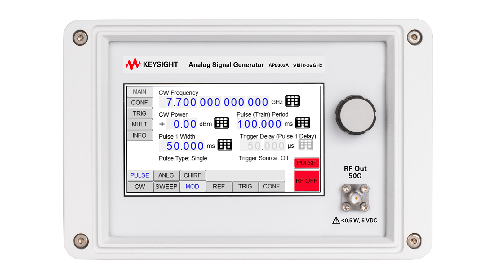
条件:1. Rotary Knob changes the value selected on the screen.
2. RF 50 Ω Output connector SMA-female
1. Trigger input BNC female
2. Function output BNC female
3. External reference input BNC female
4. Internal reference output BNC female
5. FM/PM modulation input BNC female
6. AM and Pulse modulation BNC female
7. LAN connection RJ-45
8. USB 2.0 device
9. GPIB Port
10. DC Power plug (6V, 6 A)
11. DC power switch
12. Ground Screw
13. Fan Holes (air intake)
14. Fan Holes (air exit)
1. Trigger input BNC female
2. Function output BNC female
3. External reference input BNC female
4. Internal reference output BNC female
5. FM/PM modulation input BNC female
6. AM and Pulse modulation input BNC female
7. LAN connection RJ-45
8. USB 2.0 device
9. GPIB Port
10. Ground Screw
Front (3U Housing)
Rear (3U Housing)
Front (Option S1E
1U Housing)
19” rack-mount module, SMA RF output connector
Rear (Option S1E
1U Housing)
External Power Bank Adapter Cable (3U Housing Only)
The Y9614A (# 1 above) is designed to power the 3U AP5001A or AP5002A (#
2 above) from an
external, customer supplied, power bank (#
3 above) with output voltage of 12V to 25V. Power bank
capacity of 50 Ah is recommended and it should be equipped with a barrel connector per below
specifications with a maximum output current of 7 A.
The Y9614A has two connectors marked as ‘Input’ and ‘Output’. The output connector is directly
connected to the DC
6.3V input port on the rear of an AP5001A or AP5002A. The input connector is
Input connector Barrel connector 2.1 x
5.5 mm, outer sleeve negative Connected to power bank
Output connector Barrel connector 2.1 x
5.5 mm, outer sleeve negative Connected to AP5001A/2A
Input voltage range
12 V to 25 V DC
Input power consumption Typ.
36 W
Cooling To ensure sufficient passive cooling, air circulation
Ethernet
100BaseT LAN interface
Control language SCPI Version
1999 compatible
Power requirements 6.3 ± 0.2 VDC
30 W maximum
S1E)
100-240 VAC, 50-60 Hz
42 W max
Mains adapter supplied (except option S1E) 100-240 VAC in/ 6.3 V
5.71 A DC out
条件:altitude, and power line conditions.
Environmental stress Samples of this product have been type tested to
be robust against the environmental stresses of storage, transportation,
and end-use; those stresses to temperature, humidity, shock, vibration,
Storage temperature range
–40 to 70 °C
Operating temperature range
0 to 55 °C
0 to 45° C with option S1E
40 °C for Y9614A
Max. Relative Humidity
85% up to 45 °C ambient (40 °C for Y9614A)
Operating and storage altitude up to 15,000 feet
EMC complies and EMC regulations and directives for emission and
immunity to interference (EN 61326-1 Industrial, EN/IEC
61326-2-1)
Safety complies with applicable Safety regulation in line with IEC/EN
61010-1
Weight Weight ≤ 4.3 kg (9.5 lbs) net, ≤
5.4 kg (12 lbs) shipping
Weight S1E ≤ 6 kg (13.23 lbs) net, ≤
8 kg (17.63 lbs) shipping
Weight (Y9614A empty) ≤
0.167 kg (0.37 lbs) net
Dimensions Including connectors: W x L x H = 174 x 262 x
117 mm
Dimensions (Option S1E) W x L x H = 426 x 460 x 42 mm [16.8 x 18.1 x
1.7 in]
Recommended calibration cycle
24 months
Keysight enables innovators to push the boundaries of engineering by quickly solving
design, emulation, and test challenges to create the best product experiences. Start your
This information is subject to change without notice. © Keysight Technologies, 202
4 - 2026
Published in USA, July 24 , 202 6, 312
4-1576 .EN
型号/选件说明 Additional Information
AP5002A RF Microwave Signal Generator
AP5002A-512 Frequency range
9 kHz to 12 GHz
AP5002A-520 Frequency range
9 kHz to 20 GHz
AP5002A-526 Frequency range
9 kHz to 26 GHz
AP5002A-1E1 Step attenuator
AP5002A-1EA High output power
AP5002A-UNQ Band limited fast switching not license upgradeable
AP5002A-UNZ Fast switching not license upgradeable
AP5002A-GPB GPIB interface not license upgradeable
AP5002A-S1E
1U rack-mount module not license upgradeable
AP5002A-1EM Move RF output to rear panel Requires Option S1E, not license
AP5002A-UK6 Commercial calibration certificate with test data
AP5002A-MDH
1 MΩ FM/PM input impedance not license upgradeable
Y9612A Portable bag
Y9614A External power bank adapter cable with voltage
For use with customer supplied power bank
AP5002AU-F01 Frequency upgrade from 12 GHz to 20 GHz License key only
AP5002AU-F02 Frequency upgrade from 12 GHz to 26 GHz License key only
AP5002AU-F03 Frequency upgrade from 20 GHz to 26 GHz License key only
AP5002AU-1E1 Add step attenuator License key only
AP5002AU-1EA Add high output power License key only
以上指标摘自厂家官方数据手册,完整定义、测试条件与保证值口径以手册为准。完整指标、测试条件与定义口径请见产品页「软件和手册 | 白皮书」栏目中的官方数据手册。
是德科技 | KEYSIGHT · onetest 仪器资源库


 客服









 粤公网安备44030902003758