是德科技 | KEYSIGHT
XG5系列N5186A 9kHz 至3/6/8.5 GHz 1/2/3/4多通道矢量信号发生器 250/500/960MHz带宽 详细指标
矢量信号发生器
Internal I/Q baseband generator adjustments
23
Internal I/Q offset Separate I and Q offsets
± 20%
Internal I/Q quadrature angle
± 20°
Internal I/Q gain balance
± 10 dB
Internal I/Q time skew
± 83.3333 ns
I/Q common delay range
0 to 41.6667 ns
I/Q common delay resolution
250 fs
Type Single ended, differential
条件:Amplitude flatness ± 0.2 dB measured with channel corrections optimized for I/Q output
Phase flatness ± 2.5 degrees measured with channel corrections optimized for I/Q output
Output impedance Single-ended
50 ohm per output
Differential
100 ohm per output
Maximum voltage per output 2V peak (into
50 ohms)
Bandwidth (I,Q) Baseband (I or Q) 50% of available modulation bandwidth
24
RF (I + Q) 100% of available modulation bandwidth
24
Common mode I/Q offset ± 1.5V into 50 ohms (50 uV resolution) <
380MHz baseband bandwidth
± 0.30V into 50 ohms (50 uV resolution) >
380MHz baseband bandwidth
Differential mode I or Q offset ± 2V into 50 ohms (50uV resolution) <
380MHz baseband bandwidth
± 1V into 50 ohms (50uV resolution) >
380MHz baseband bandwidth
None (direct digital modulation, no I/Q modulator)
条件:Frequency range Amplitude Phase 400 MHz to 8.5 GHz ± 0.6 dB ± 5° 23 I/Q adjustments represent user interface nominal parameter ranges and not specifications. 24 See RF (I + Q) bandwidth and sample rate for available modulation bandwidth.
Frequency response over available modulation bandwidth24, measured
User defined automatic channel response correction and S-parameter de-embedding (E7653APPC)
Methods for fixture error removal
Scatter parameters de-embedding/embedding files generated by a network analyzer or simulation
Automatic channel response correction using a power sensor or spectrum analyzer (amplitude and phase correction)
File format .s2p, .csv
Number of cascadable calibration sets
4
Automated channel response correction (256 taps)
25
Recommended maximum amplitude for error correction
± 5 dB across modulation bandwidth
Entry modes USB or LAN direct power meter control 25 Automated routine uses power sensor to correct for linear amplitude response of DUT (equalizer). See
User Documentation for more details
-1.00
-0.50 0.00 0.50 1.00
-500 -400 -300 -200 -100 0 100 200 300 400
500
Measured Amplitude Flatness, 0 dBm, 1 GHz Bandwidth 2 GHz
3 GHz
4 GHz
5 GHz
6 GHz
-10
-5
-500 -400 -300 -200 -100 0 100 200 300 400
500
Measured Phase Flatness, 0 dBm, 1 GHz Bandwidth 2 GHz
3 GHz
4 GHz
5 GHz
6 GHz
Signal Each channel can generate one signal (ex: one waveform file).
Internal baseband generator (Options BxX / Rxx)
I/Q file resolution
16 bits
Waveform granularity
1 sample
Signal attenuation
0 to -100 dB
Sample rate resolution
1 Hz
Interpolated I/Q rate
1.2 GHz
RF (I + Q) bandwidth
26 and sample rate
选件 RF (I + Q) 带宽 (nom) 采样率 (nom)
Option B5X 500 MHz
600 MHz
Option B9X / R10 27 1 GHz
1.2 GHz
最大值 arbitrary 波形 playback 存储
Maximum storage capacity
256 GB (nom)
Quantum: See Waveform granularity
Minimum memory allocation blocking factor
64 Bytes or 16 samples
Maximum number of waveform files >
1000, depending on available memory
条件:27 1 GHz RF bandwidth applies to option B9X with firmware version A.16.00 or later.
Maximum number of segments per sequences
65,280
Maximum number of repetitions 232
-1
26 Lower edge of modulated signal is not recommended to extend below
10 MHz. Upper edge of modulated signal is
not recommended to extend above
8.5 GHz.
Multi-channel baseband synchronization primary/secondary (Option PCH and SNC)
Global trigger delay range
0 µs to 6.82 µs
Global trigger delay resolution
± 1.67 ns
Global trigger jitter
± 1.67 ns
Channel-to-channel relative trigger repeatability <
± 5 ps
Markers are defined in a segment during the waveform generation process, or from the front panel; see User Documentation or O nline Help for
Marker polarity Positive, negative
Modes of operation Standalone signal or digitally added to signals
Crest factor
12.9 dB (nom)
Randomness
16.3 hours (nom)
Carrier-to-noise ratio
± 100 dB when added to signal
Carrier-to-noise ratio formats C/N, Eb/No
CW interferer (Option
403)
Modes of operation Standalone signal or digitally added to signals
Frequency offset ± half of maximum baseband bandwidth
28
28 For maximum baseband bandwidth and sample rate, see RF (I + Q) bandwidth and sample rate .
Segment advance Not supported
External delay time
0 to 41s (nom)
External delay resolution
833 ps (nom)
I/Q delay range See Internal I/Q baseband generator adjustments section
I/Q delay resolution See Internal I/Q baseband generator adjustments section
Multitone and single tone (E7621APPC)
Number of tones Multitone mode
2 to 200,001
Tone spacing 100 Hz to Floor [(maximum baseband bandwidth 30)/((number of tones) - 1)/100] *
100
Multi-Instrument Synchronization (Option SNC)
Multi-instrument synchronization mechanism
31
Number of endpoints Up to 4
工作模式(含) leader, independent
条件:available leader outputs, a power splitter or distribution amplifier may be required. See Startup Guide for input/output power level requirements.
An endpoint is defined as a single N5186A instrument, regardless of channels in the instrument.
Multi-instrument synchronization configurations
31
The leader instrument must be able to supply the required inputs to each follower. For configurations where the number of req uired follower inputs exceeds the
Basic multi-instrument synchronization
Hardware Configuration Number of available outputs as a leader
Channels Maximum frequency Endpoints 2.4 GHz
2.4 GHz
3, 6, or 8.5 GHz
002)
003, and 004)
29 Single tone generates a single CW tone at a specified offset to the channel’s RF frequency.
30 For maximum baseband bandwidth and sample rate, see RF (I + Q) bandwidth and sample rate .
31 Compatible with serial prefix breaks MY6436xxxx or higher.
EVM performance data 32, temperature range
20 to 30 °C
Format GSM LTE FDD 802.11a/g 802.11ac QPSK
16QAM
Modulation type GMSK (bursted) 64 QAM 64 QAM 256 QAM QPSK
16 QAM
Modulation rate 270.833 ksps 10 MHz BW 54 Mbps 80 MHz 4 Msps (root-Nyquist filter α =
0.25)
Configuration 1 timeslot E-TM
3.1 - - - -
Frequency 33
800 to 900 MHz
1800 to1900 MHz 1800 to 2200 MHz
2400 to 2484 MHz
5150 to 5825 MHz 5.775 GHz ≤ GHz
3
≤ 6 GHz
≤ 3 GHz
≤ 6 GHz
Power level dBm
-10 dBm to +7
-20 dBm to +7
dBm -18 dBm to -5 dBm -15 dBm to -5 dBm dBm
-10 dBm to +4
-10 dBm to +4 dBm
Power level with option
1EA
-10 dBm to +10 dBm
-20 dBm to +10 dBm
-18 dBm to +2 dBm
-15 dBm to +2 dBm
-10 dBm to +5 dBm
-10 dBm to +5 dBm
条件:32 EVM specifications apply for the default ARB file setup conditions with the default ARB files supplied with the instrument.
Spec Typ Typ Meas Meas Spec Spec Spec Spec rms 0.8° 0.2° 0.2% 0.2% 0.36% 0.8% 1.1% 0.65%
0.9%
EVM for 5G NR FR1 bands
-10 dBm to +5 dBm, () = typical
Frequency 100 MHz, 256 QAM, 60 kHz SCS, NRB =
135
2 GHz (0.25%)
3.55 GHz (0.27%)
4.5 GHz (0.29%)
33 Performance evaluated at bottom, middle, and top of bands shown. WLAN 802.11ac 80 MHz, 256 QAM, MCS
7 symbols, no
filtering. Channel corrections
-55
-50
-45
-40
-35
-30 -25 -20 -15 -10 -5 0 5
10
Measured EVM peformance vs. power
WLAN 802.11be @7 GHz, 320 MHz, MCS13
300 µs
Distortion Performance (ACPR) 3GPP W-CDMA distortion performance, temperature range
20 to 30 °C, () = typical
Power level
-12 dBm to +2 dBm
34 -12 dBm to + 2 dBm 19 -12 dBm to +5 dBm
19
Offset Configuration Frequency Standard Option UNV Option UNV with
Adjacent (5 MHz)
1 DPCH, 1 carrier
1800 to 2200 MHz
(-71 dBc) (-73 dBc) (-73 dBc)
Alternate (10 MHz) (-72 dBc) (-74 dBc) (-74 dBc)
Adjacent (5 MHz) Test model
1 with
64 DPCH, 1 carrier
1800 to 2200 MHz
(-70 dBc) (-72 dBc) (-72 dBc)
Alternate (10 MHz) (-71 dBc) (-73 dBc) (-73 dBc)
3GPP LTE-FDD distortion performance, temperature range
20 to 30 °C, () = typical
Power level -10 dBm to +2 dBm -10 dBm to +2 dBm
-10 dBm to +5 dBm
Offset
35 Configuration Frequency Standard Option UNV Option UNV with
Adjacent (10 MHz) 10 MHz E-TM
1.1
-64 dBc -67 dBc (-69 dBc)
-67 dBc (-69 dBc)
Alternate (20 MHz) -66 dBc -69 dBc (-71 dBc)
-69 dBc (-71 dBc)
GSM output RF spectrum (ORFS) distortion performance, temperature range
20 to 30 °C, () = typical
Power level
-10 dBm to +7 dBm
Offset Configuration Frequency
36 Standard Option UNV
200 kHz
1 normal timeslot,
bursted 800 to 900 MHz
1800 to 1900 MHz (-33 dBc) (-35 dBc)
400 kHz (-68 dBc) (-70 dBc)
600 kHz (-81 dBc) (-84 dBc)
800 kHz (-82 dBc) (-84 dBc)
1200 kHz (-84 dBc) (-86 dBc)
5G NR FR1 bands distortion performance, -10 dBm to +5 dBm, temperature range
20 to 30 °C, () = typical
Adjacent (100 MHz)
60 kHz SCS,
NRB =135
2 GHz
-58 dBc (-60 dBc)
Alternate (200 MHz)
-59 dBc (-61 dBc)
Adjacent (100 MHz)
3.55 GHz
-58 dBc (-60 dBc)
Alternate (200 MHz)
-55 dBc (-57 dBc)
Adjacent (100 MHz)
4.5 GHz
-55 dBc (-57 dBc)
Alternate (200 MHz)
-57 dBc (-59 dBc)
Adjacent (100 MHz)
5 GHz
-56 dBc (-58 dBc)
Alternate (200 MHz)
-56 dBc (-58 dBc)
34 This is rms power. Convert from rms to peak envelope power with the following equation: PEP = rms power + crest factor (for
example, 3GPP test model 1 with 64 DPCH has a crest factor 11.5 dB, therefore at +5 dBm rms, the PEP = 5 dBm +
11.5 dB =
+16.5 dBm PEP).
35 ACPR measurement configuration: reference channel integration BW: 9.015 MHz, offset channel integration BW
9.015 MHz.
36 Performance evaluated at bottom, middle, and top of bands shown.
-78
-76
-74
-72
-70
-68
-66
-64
-62
-60
Measured 10 MHz LTE E-TM
1.1 QPSK ACPR
Adjacent (10 MHz offset) Alternate (20 MHz offset)
-66
-64
-62
-60
-58
-56
-54
-52
-50
-48
-20-18-16-14-12-11-10 -9 -8 -7 -6 -5 -4 -3 -2 -1 0 1 2 3 4 5 6 7 8 9
10
Measured 5G FR1 SCS60
100 MHz ACPR
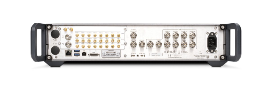
RF output Outputs the RF signal via a precision Type-N female connector; see output section for reverse power
USB
2.0 Type-A connector used with a memory stick for transferring instrument states, licenses and other files
into or out of the instrument
USB 3.0 Outputs
2 A at 15 V.
条件:Rear panel inputs and outputs are 3.3 V CMOS, unless indicated otherwise; CMOS inputs will accept 5 V CMOS, 3 V CMOS, or TTL voltage levels.
nominal input impedance. Selectable DC- or AC- coupling. Damage levels are ±5 V.
nominal input impedance. Selectable DC- or AC- coupling. Damage levels are ±5 V.
1 channel configuration Outputs the RF signal via a precision Type-N female connector
2 channel configuration Outputs the RF signal via a precision Type-N female connector
4 channel configuration Outputs the RF signal via a
3.5 mm female connector
EXT1 In BNC connector accepts analog input signal for AM, FM, and ΦM. Selectable 50 Ω, 600 Ω
100 kΩ
EXT2 In BNC connector accepts analog input signal for AM, FM, and ΦM. Selectable 50 Ω, 600 Ω
100 kΩ
Channel 1 BNC connector. The marker signal can also be routed internally to
Channels 2-4 SMB connector; only events
1-2. The marker signal can also be
routed internally to control the RF blanking
Channel 1 BNC connector. Accepts CMOS signal with minimum pulse width of
10 ns. Damage levels are > +5.5 V and <
–2 V.
SMB connector, only triggers
1-5. Accepts CMOS signal with
minimum pulse width of 10 ns. Damage levels are >
+5.5 V and
< –2 V.
条件:BNC connector; see Internal Pulse Generator table for more information. Input threshold 0.5 V nominal. Damage levels are > +5
SMB connector; see Internal Pulse Generator table for more information. Input threshold 0.5 V nominal. Damage levels are > +5
LF OUT / SWEEP OUT BNC connector outputs the internal analog modulation source signal. -1V to +5V nominal output into 50
Ω. Nominal 50 Ω output impedance.
条件:Option 1ER add the capability to lock to a frequency from 1 MHz to 110 MHz; nominal input level –3 to
dBm; nominal output impedance 50 Ω.
BNC connector; accepts a
10 MHz reference signal used to frequency lock the internal timebase. Input
+20 dBm, impedance
50 Ω, sine or square waveform.
10 MHz out (Ref Out) BNC connectors outputs the 10 MHz reference signal used by internal timebase; level nominally
+3.9
Type-A Copy files to and from removable storage devices
Type-B Provides remote programming functions via SCPI over USBTMC/
USB488.
LAN (1000 BaseT)
The LAN connector provides the same SCPI remote programming functionality as the GPIB connector
and is also used to access the internal Web server and FTP server.
Supports DHCP, sockets SCPI, VXI-11 SCPI, connection monitoring, dynamic hostname services, TCP
VXI-11 HiSlip SOCKET USB-488
USB Version-488
Control languages Control languages SCPI Version
1997.0
Keysight’s IO Library Suite helps you quickly establish an error-free connection between your PC and
instruments – regardless of the vendor. It provides robust instrument control and works with the software
条件:Maximum relative humidity (non-condensing) 95%RH up to 40 °C, decreases linearly to 45%RH at 55 °C
Operating 1 channel 0 to 55 °C 2 channel 0 to 50 °C 4 channel
0 to 50 °C
Operating and storage altitude Up to 4,600 meters
条件:and power line conditions; test methods are aligned with IEC 60068-2 and levels are similar to
Samples of this product have been type tested in accordance with the Keysight Environmental Test
Manual and verified to be robust against the environmental stresses of storage, transportation and
enduse; those stresses include but are not limited to temperature, humidity, shock, vibration, altitude,
Complies with European Low Voltage Directive
2006/95/EC
Canada: CSA C22.2 No.
61010-1
条件:Cet appareil ISM est conforme a la norme NMB- 001 du Canada. 37 AC line voltage dropouts (IEC 61000 -4-11) of duration greater than 5 ms will cause the RF output to turn off until it is re -enabled by the operator, in order to protect internal hardware.
Complies with European EMC Directive
2004/108/EC
IEC/EN 61326-1or IEC/EN
61326-2-1 CISPR Pub
11 Group 1, class A AS/NZS CISPR
11
ICES/NMB-001
2This ISM device complies with
Canadian ICES-001.
Configuration 1 channel (001) 2 channel (001/002)
4 channel (001/002/003/004)
Weight 16.09 kg (or 35.47 lbs) 17.9 kg (39.46 lbs) 21.73 kg (or
47.91 lbs)
Height 88.25 mm (without feet)
102 mm (with feet)
Width with handles
474.7 mm
Width without handles
425.5 mm
Length with handles (including connectors)
591.1 mm
Length without handles (including connectors)
501.9 mm
Recommended calibration cycle
1 year
Number of channels Maximum frequency Power requirements Average power consumption
650 W Max
270 W nom.
2 (opt. 001, 002) 3/6/8.5 GHz (opt.
503/506/508)
650 W Max
380 W nom.
4 (opt. 001, 002, 003, and 004) 3/6/8.5 GHz (opt.
503/506/508)
650 W Max
550 W nom.
Internal Removable solid-state drive (256 GB)
External Supports USB
3.0/2.0 compatible memory devices
One year of KeysightCare Assured is included with your new N5186A MXG Vector Signal Generator for
priority access to technical experts and optimized uptime to mitigate project risk. Multiyear upgrade
options to KeysightCare Enhanced add calibration coverage for full performance verification and
accelerated turnaround times
Obtain multi-year KeysightCare upfront to lock in the service pricing of today and operate with a planned
spending profile and eliminate the need for yearly requests for maintenance budget. Plus, you benefit
from secured service for
3, or 5 years.
KeysightCare Enhanced
38 Includes tech support, warranty, and calibration
R-55B-001-1 KeysightCare Enhanced – Upgrade
1 year
R-55B-001-2 KeysightCare Enhanced – Extend to 2 years
R-55B-001-3 KeysightCare Enhanced – Extend to 3 years (Recommended)
R-55B-001-5 KeysightCare Enhanced – Extend to 5 years (Recommended)
R-55B-001-3CC KeysightCare Enhanced – Extend to 3 years (China only)
39
R-55B-001-5CJ KeysightCare Enhanced – Extend to 5 years (Japan only)
KeysightCare Assured Includes tech support and warranty
R-55A-001-2 KeysightCare Assured – Extend to 2 years
R-55A-001-3 KeysightCare Assured – Extend to 3 years
R-55A-001-5 KeysightCare Assured – Extend to 5 years
R-55A-001-3CC KeysightCare Assured – Extend to 3 years (China only)
R-55A-001-5CC KeysightCare Assured – Extend to 5 years (China only)
R-55A-001-5CJ KeysightCare Assured – Extend to 5 years (Japan only)
条件:and test so customers can solve the world’s most complex engineering challenges.
PS-S20 Startup assistance, daily
PS-X10 Custom Services
38 Available in select countries. R-55B-001-2/3/5 must be ordered with R-55B-001-1. For details, please view the KeysightCare
datasheet.
39 Contact Keysight for 5 year coverage.
As a mission -critical design enablement partner, Keysight connects design, emulation,
This information is subject to change without notice. © Keysight Technologies, 202 3 - 202
6
Published in USA, October 3 , 202 6, 3123
-1690 .EN
Publication title Publication number
N5186A MXG Configuration Guide
3123-1623EN
以上指标摘自厂家官方数据手册,完整定义、测试条件与保证值口径以手册为准。完整指标、测试条件与定义口径请见产品页「软件和手册 | 白皮书」栏目中的官方数据手册。
是德科技 | KEYSIGHT · onetest 仪器资源库


 客服









 粤公网安备44030902003758