是德科技 | KEYSIGHT
UXG系列N5192A 50MHz至20GHz捷变矢量适配器,改进型 详细指标
精准模拟复杂信号场景
Specified range Tunable range
条件:N5194A with option 520 50 MHz to 20 GHz 10 MHz to 20 GHz
N5194A with option 540 50 MHz to 40 GHz 10 MHz to 44 GHz
N5192A with option 52E 50 MHz to 20 GHz 10 MHz to 20 GHz
CW frequency resolution
0.001 Hz
Adjustable in 0.1° increments
条件:1. RF CW switching speed using an external hardware trigger. Speeds apply for any combination of frequency, amplitude ≤ max specified power and phase
Accuracy is equivalent to the external frequency reference in use.
External
6 GHz reference input
Input amplitude
+5 to +15 dBm (nom)
Input impedance
50 Ω (nom)
Lower band 10 MHz to <
20.000000016 GHz
– Main lower band 50 MHz to <
20.000000016 GHz
– Extended lower band 10 MHz to <
50 MHz
Upper band
20.000000016 GHz to 44 GHz
– Main upper band 20.000000016 GHz to <
40 GHz
– Extended upper band
40 GHz to 44 GHz
Switching speed for N5194A
1
Main lower band Main upper band 40 GHz20.000000016 GHz 44 GHz10 MHz
50 MHz
Within lower band Within main lower band 3 2.5 3.5
3.5
Other transitions 3 2.5
3.5 —
Within upper band Within main upper band
4.5 — —
Within upper sub–bands 3 3
2.5 — —
Between main lower and main upper bands 5.5
5 — —
Other transitions 5.5
5 — —
RF phase settling criteria
Final frequency 10 MHz to < 2.85 GHz Measured to phase settled within 0.1 radians of final phase 2.85 GHz to < 8.64 GHz Measured to phase settled within 0.2 radians of final phase 8.64 GHz to < 17.3 GHz Measured to phase settled within
0.3 radians of final phase
≥ 17.3 GHz Measured to phase settled within
0.4 radians of final phase
Update rate (Transition time)
1
Within lower band Within Main Lower band 250 ns (190 ns) 220 ns (170 ns)
740 ns (470 ns) (210 ns)
Other transitions (250 ns) (220 ns) (250 ns) —
Within 上限频段 Within Main 上限
Band 4.5 µs (2.5 µs)
4.5 µs (2.5 µs) — —
Within upper sub–bands
3 (250 ns) (220 ns) — —
Other transitions (3.3 µs) (3.3 µs) — —
条件:1. Update Rate is determined by the transition time as measured from the start of the RF transition (where the frequency, amplitude and phase are undefined) to
RF amplitude and phase settled. Latency is measured from the input trigger to RF amplitude and phase settled.
2. Optimized Mode applies when switching start frequency is not within any of the following 3 zones: (0 to 2.5 GHz) or (6.5 to 8 GHz) or (10 to 11.5 GHz), or stop
frequency is not within any of the following 2 zones: (13 to 14 GHz) or (18.5 to 20 GHz).
3. Upper sub bands include: 20.000000016 GHz to < 24.0 GHz
Upper Bands 7 µs (4.3 µs)
7 µs (4.1 µs) — —
Other transitions (8 µs) (8 µs) — —
43.3 GHz to 44 GHz
条件:2. The N5192A does not have specified phase repeatability.
Figure
1. Switching speed definitions with input trigger
Switching speed for N5192A
2
External LO mode, narrowband, nom External LO mode, wideband, nom
Update rate (transition time between pulses in streaming) 101 µs 101 µs 1. For streaming mode only. Update rate refers to the transition time from the finishing of the leading pulse to the phase and amplitude settled in the following
pulse. The diagram in N5194A section doesn’t apply.
Additional contributors to switching speed
With LAN or USB control Add
900 µs (nom) from receipt of SCPI command
RF phase settling criteria
Final frequency 10 MHz to < 2.85 GHz Measured to phase settled within 0.1 radians of final phase 2.85 GHz to < 8.64 GHz Measured to phase settled within 0.2 radians of final phase 8.64 GHz to < 17.3 GHz Measured to phase settled within
0.3 radians of final phase
≥ 17.3 GHz Measured to phase settled within
0.4 radians of final phase
RF amplitude settling criteria 50 MHz to 40 GHz Measured to amplitude settled to within
1 dB of final amplitude
Option
520 or 52E Max available power Max specified power
Internal LO mode, dBm spec 10 MHz to < 2.5 GHz +6 (+7) +6 (+7) +3 +3 2.5 GHz to 4 GHz +7 (+8) +6 (+9) +3
+3
> 4 GHz to 14 GHz +7 (+10) +4 (+7) +3
+3
> 14 GHz to 18 GHz +6 (+8) +6 (+8) +3
+3
> 18 GHz to 20 GHz +1 (+4) –1 (+3) +1
–2
Option
540 Max available power Max specified power
条件:1. Maximum CW power specifications are warranted from 15 to 40 ˚C. Maximum power in the 40 to 50 ˚C temperature range typically degrades less than 1 dB.
2. Instrument specifications are based on max specified power, unless otherwise stated. When operating at max available power, spectral purity will be
Internal LO mode, dBm spec 10 MHz to < 2.5 GHz +5 (+7) +5 (+7) +3 +3 2.5 GHz to 4 GHz +5 (+8) +5 (+7) +3
+3
> 4 GHz to 14 GHz +5 (+7) +4 (+6) +3
+3
> 14 GHz to 18 GHz 0 (+3) 0 (+3) 0
0
> 18 GHz to 20 GHz –4 (0) –4 (0) –4
–4
> 20 GHz to 35 GHz –2 (+1) N/A
–2 N/A
> 35 GHz to 40 GHz –5 (–1) N/A
–5 N/A
Figure
2: Maximum CW power (measured).
Maximum power, Option
520 or 52E
条件:1. CW power accuracy specifications are warranted from 0 to 50 ˚C. Specifications apply within ± 3 ˚C of last power alignment. Temperature compensation is
ON. If temp comp is OFF, amplitude drift will be ≤ 0.2 dB/˚C. For instruments with Option 1ED Type–N connectors, specifications apply below 18 GHz and
2. Specifications apply in vector mode only, over a power range of –5 to –85 dBm.
Frequency (MHz) 0 2000 4000 6000 8000 10000 12000 14000 16000 18000
20000
Maximum power, Option
520 or 52E
performance is typically degraded 0.2 dB above
18 GHz.
–120 dBm
Attenuator range
0 to 65 dB in 5 dB steps
Frequency Output power, dBm External LO mode, dB spec (typ) Internal LO mode, dB spec (typ)
50 MHz to 14 GHz Max specified power to –90 dBm ± 1.00 (± 0.33) ± 1.00 (
± 0.34)
0 to –120 dBm ± 1.65 (± 0.41) ± 1.65 (
± 0.45)
> 14 GHz to 20 GHz Max specified power to –10 dBm ± 0.80 (± 0.20) ± 0.65 (
± 0.2)
–10 to –90 dBm ± 1.05 (± 0.33) ± 1.00 (
± 0.27)
–10 to –120 dBm ± 1.75 (± 0.50) ± 1.85 (
± 0.47)
> 20 GHz to 40 GHz Max specified power to –50 dBm ± 1.00 (
± 0.50) N/A
–50 to –80 dBm ± 1.20 (
± 0.60) N/A
Frequency Output power, dBm External LO, dB spec (typ) Internal LO, dB spec (typ)
50 MHz to 18 GHz +3 to –25 ± 2.5 (± 0.4) ± 2.5 (
± 0.4)
200 MHz to 18 GHz < –25 to –75 ± 2.5 (± 0.4) ± 2.5 (
± 0.4)
700 MHz to 18 GHz < –75 to –90 ± 2.5 (± 0.5) ± 2.5 (
± 0.5)
> 18 GHz to 20 GHz +1 to –25 ± 2.5 (
± 0.5) N/A
–2 to –25 N/A ± 3.0 (
± 0.5)
< –25 to –75 ± 2.5 (± 0.5) ± 2.5 (
± 0.5)
< –75 to –90 ± 2.5 (± 0.5) ± 3.0 (
± 0.6)
> 20 GHz to 40 GHz Max specified power to –50 dBm
± 2.5 (+0.5) N/A
Frequency 0 dB atten ≥
5 dB atten
50 MHz to 18 GHz 1.6:1
1.6:1
> 18 GHz to 20 GHz 1.9:1
1.6:1
> 20 GHz to 40 GHz 2.0:1
2.0:1
Phase linearity vs. power
2
Frequency 50 MHz to 16 GHz
1.0 deg RMS (nom)
> 16 GHz to 40 GHz
2.0 deg RMS (nom)
条件:configured as the LO controller and it is typically connected to the N5193A via a 100 pin LVDS cable.
Multiple UXG agile vector adapters can be synchronized together with one UXG agile signal generator to have coherent outputs. This
is useful for simulating angle–of–arrival (AoA) and phased array antenna wavefronts. One of the UXG vector adapter units must be
Synchronization input connections
条件:wide variety of input frequencies. See the Rear Panel Connectors section for connection details.
Connectors section for connection details. 6 GHz input Provides high stability synchronization between multiple signal generators. This is not a general 6 GHz connection. Only the 6 GHz synchronization output from another compatible signal generator should be connected. See the Rear Panel Connectors section for connection details.
System Sync input Recommended external reference input for use in system environments where trigger jitter and phase stability are important. Accepts a
System Sync output Provides a buffered version of the signal provided to the System Sync input for use in multi–instrument systems. See the Rear Panel
6 GHz output Provides high stability synchronization between multiple N519xA UXG signal generators. See the Rear Panel Connectors section for
条件:LO input Input port for external LO signal when operating in External LO mode. Normal input range is 8 to 20 GHz with ≥ +5 dBm (nom) power.
50 Ω (nom) impedance.
Internal LO mode (N5194A only)
Frequency tuning is accomplished with an internal LO signal. No external LO signal is needed in this mode, but an external
6 GHz reference
signal is still required. When using the Internal LO, the N5194A will only operate in standard vector mode and cannot be operated in wideband
vector mode. Note that performance characteristics in this data sheet are based on using the Keysight N5193A UXG agile signal generator
to provide the
6 GHz reference signal. Other signal generators can be used to provide the reference signal, but system performance will be
unspecified. Internal LO mode operation is available up to 20 GHz only. This can only be done in vector mode, not enhanced vector mode or
External LO mode (N5194A and N5192A)
The LO signal is provided by an external source. An external
6 GHz reference signal is also required. Note that performance characteristics
in this data sheet are based on using the Keysight UXG agile signal generator to provide both the external LO as well as the
6 GHz reference
signals. Other signal generators can be used to provide the LO and reference signals, but system performance will be unspecified. External LO
mode operates over the full frequency range of the instrument. The N5194A can be used as an External LO for the N5193A, and the N5192A
can be used as an External LO for the N5191A.
条件:asynchronously, based on the time stamp information contained within the PDW.
Dual Arb This feature plays arbitrary I/Q waveforms. Four markers are associated with each I/Q sample consisting of a pair of 16-bit words.
By adding the optional N5194326A 1 real-time pulse generation capability, the following can be coded in the PDW and generated in real time:
1. N5194326A real–time pulse generation is subject to US ITAR export controls. For more information, please contact your Keysight representative.
– N5194A PDW streaming is a standard feature that provides agile control of most of the instrument settings with a continuous stream of PDWs transferred
from the internal SSD or an external source, such as a LAN. Each PDW has a Pulse Start Time. The scenario starts playing at time
0 (or a
specified offset time). The scenario runs until the end of the simulation (either the end of an internal file or when the external connection is closed
with LAN). The simulation can run forever from LAN if the Scenario Time reset feature is used. The streaming PDW parameters are executed
– N5192A PDW streaming is an optional feature enabled by adding the N5192ST1A PDW streaming capability. The N5192ST1A enables the same PDW
streaming capabilities as described above for the N5194A.
Real-time PDW streaming (N5194A only)
unmodulated rectangular CW pulses, PSK/FSK modulated pulses, and pulses with linear chirp (up/down/triangle). This makes it possible to
continuously stream PDWs without the need to reference waveform segments in baseband generator memory. The minimum time between
real-time pulses is
240 ns.
条件:1. Measured using a CW signal with power set to –10 dBm and 0 dBm or max specified power, whichever is lower. Performance is unspecified for harmonics
beyond the specified frequency range. Harmonic specifications are warranted from 15 to 40 ˚C.
2. The –10 dBm harmonic specifications are applicable over a 110 dB agile dynamic range.
3. Does not apply to N5192A UXG vector adapter, modified version.
Fundamental frequency Harmonic level (dBc) at ≤
–10 dBm Harmonic level (dBc) at 0 dBm or max
available power, whichever is lower 10 MHz to < 50 MHz (–32) (–32) 50 MHz to 500 MHz –30 (–33)
–30 (–33)
> 500 MHz to 800 MHz –51 (–56)
–52 (–56)
> 800 MHz to 4 GHz –60 (–65)
–56 (–62)
> 4 GHz to 8 GHz –64 (–69)
–58 (–63)
> 8 GHz to 12.5 GHz –66 (–72)
–61 (–66)
> 12.5 GHz to 20 GHz –59 (–65)
–53 (–58)
> 20 GHz to 22 GHz (–68) (–59)
External LO mode, wideband or enhanced vector mode (Opt BB1 or BB2)
Fundamental frequency Harmonic level (dBc) at ≤
–10 dBm Harmonic level (dBc) at 0 dBm or max
available power, whichever is lower 10 MHz to < 50 MHz (–32) (–32) 50 MHz to 2 GHz –30 (–33)
–30 (–33)
> 2 GHz to 3 GHz –24 (–28)
–20 (–24)
> 3 GHz to 4 GHz –31 (–35)
–29 (–33)
> 4 GHz to 8 GHz –63 (–69)
–58 (–63)
> 8 GHz to 12.5 GHz –63 (–68)
–61 (–66)
> 12.5 GHz to 20 GHz –61 (–67)
–53 (–59)
> 20 GHz to 22 GHz (–68) (–59)
Internal LO mode
3, vector mode
Fundamental frequency Harmonic level (dBc) at ≤
–10 dBm Harmonic Level (dBc) at 0 dBm or max
available power, whichever is lower 10 MHz to < 50 MHz (–32) (–32) 50 MHz to 500 MHz –30 (–33)
–30 (–33)
> 500 MHz to 800 MHz –51 (–56)
–52 (–56)
> 800 MHz to 4 GHz –60 (–65)
–56 (–62)
> 4 GHz to 8 GHz –63 (–68)
–58 (–63)
> 8 GHz to 12.5 GHz –67 (–72)
–61 (–66)
> 12.5 GHz to 20 GHz –58 (–64)
–53 (–58)
Frequency Line–related spurs at offsets ≤ 300 Hz Offsets > 300 Hz excluding line–related spurs Offsets >
10 kHz
10 MHz to <
50 MHz N/A N/A N/A
50 MHz to <
2.5 GHz (–68) (–69) (–67)
2.5 GHz to <
9 GHz (–55) (–62) (–68)
9 GHz to <
12.5 GHz (–53) (–59) (–70)
12.5 GHz to <
18 GHz (–50) (–55) (–67)
18 GHz to 20 GHz (–50) (–55) (–64)
> 20 GHz to 40 GHz (–44) (–52) (–52)
> 40 GHz to 44 GHz (–43) (–51) (–56)
External LO mode, wideband or enhanced vector mode (Opt BB1 or BB2)
Frequency Line–related spurs at offsets ≤ 300 Hz Offsets > 300 Hz excluding line–related spurs Offsets >
10 kHz
10 MHz to <
50 MHz N/A N/A N/A
50 MHz to <
1.2 GHz (–72) (–72) (–72)
1.2 GHz to <
9 GHz (–56) (–62) (–64)
9 GHz to <
12.5 GHz (–53) (–60) (–70)
12.5 GHz to 20 GHz (–49) (–55) (–64)
> 20 GHz to 40 GHz (–44) (–52) (–52)
> 40 GHz to 44 GHz (–43) (–51) (–56)
Internal LO mode
5, vector mode
Frequency Line–related spurs at offsets ≤ 300 Hz Offsets > 300 Hz excluding line–related spurs Offsets >
10 kHz
10 MHz to <
50 MHz N/A N/A N/A
50 MHz to <
2.5 GHz (–69) (–69) (–67)
2.5 GHz to <
18 GHz (–45) (–45) (–45)
18 GHz to 20 GHz (–49) (–48) (–48)
Fundamental frequency Broadband noise
3
50 MHz to 10 GHz
–140 dBc/Hz (typ)
> 10 GHz to 20 GHz
–134 dBc/Hz (typ)
条件:1. Measured using a CW signal with power set to –10 dBm. Performance is unspecified for non–harmonics beyond the specified frequency range. Non–
2. For large offsets > 4 GHz, broadband noise will drop.
3. CW signal measured with power set to +4 dBm.
4. CW signal Measured with power set to +5 dBm.
5. Does not apply to N5192A UXG vector adapter, modified version.
Fundamental frequency Broadband noise
4
50 MHz to 1 GHz
–140 dBc/Hz (typ)
> 1 GHz to 20 GHz
–125 dBc/Hz (typ)
> 20 GHz to 40 GHz
–119 dBc/Hz (typ)
harmonic specifications are warranted from 15 to 40 ˚C.
Phase Noise for N5194A
Internal LO mode for N5194A
Absolute SSB phase noise (dBc/Hz)
1
100 kHz
1 MHz
10 MHz
100 MHz
100 MHz –144 (–148) –143 (–148) –142 (–148)
–143 (–148) N/A
1 GHz –132 (–144) –132 (–143) –145 (–151) –142 (–153)
–142 (–155)
2 GHz –130 (–140) –120 (–138) –142 (–149) –143 (–150)
–143 (–150)
3 GHz –122 (–128) –126 (–132) –132 (–137) –133 (–141)
–131 (–140)
6 GHz –124 (–131) –128 (–134) –138 (–145) –141 (–148)
–138 (–146)
10 GHz –121 (–127) –125 (–131) –133 (–140) –138 (–145)
–135 (–143)
20 GHz –113 (–119) –116 (–124) –125 (–132) –127 (–135)
–124 (–133)
External LO mode for N5194A
Absolute SSB phase noise (dBc/Hz)
2
条件:1. CW signal measured with power set to +4 dBm. Phase noise specifications are warranted from 0 to 50 ˚C.
2. CW signal Measured with power set to +5 dBm. Phase noise specifications are warranted from 0 to 50 ˚C
Figure 3. Measured absolute phase noise using the internal LO mode for the N5194A.
Figure 4a. Measured absolute phase noise using the external LO mode for the N5194A.
Figure 4b. Measured absolute phase noise above 20 GHz using the external LO mode for the N5194A.
Figure 5. Measured residual phase noise using the internal LO mode for the N5194A.
Figure 6. Measured residual phase noise using the external LO mode for the N5194A.
Absolute SSB phase noise (dBc/Hz), nominal 1
spec (typ) [nom] 100 kHz spec (typ) [nom]
1 MHz
spec (typ) [nom] 10 MHz spec (typ) [nom]
100 MHz
spec (typ) [nom] 100 MHz –144 (–148) –143 (–148) –142 (–148) –143 (–148) N/A 1 GHz –132 (–144) –132 (–143) –145 (–151) –142 (–153) –142 (–155) 2 GHz –130 (–140) –120 (–138) –142 (–149) –143 (–150)
–143 (–150)
3 GHz –115 (–121) –120 (–126) –125 (–129) –123 (–131)
–121 (–129)
6 GHz –114 (–121) –117 (–124) –124 (–128) –124 (–130)
–122 (–129)
10 GHz –109 (–117) –111 (–120) –119 (–124) –118 (–126)
–118 (–128)
20 GHz –106 (–115) –108 (–118) –117 (–123) –120 (–127)
–118 (–126)
22 GHz [–117] [–121] [–126] [–129] [–130]
26 GHz [–116] [–121] [–126] [–129] [–131]
30 GHz [–117] [–121] [–126] [–129] [–129]
34 GHz [–115] [–119] [–125] [–129] [–130]
38 GHz [–115] [–119] [–125] [–127] [–122]
42 GHz [–114] [–119] [–126] [–128] [–125]
Measured internal LO absolute phase noise for N5194A
Measured external LO absolute phase noise for N5194A
-160
-140
-120
-100
-80
-60
-40
-20
11 0 100 1,0001 0,000 100,000 1,000,0001 0,000,000
100,000,000
Measured internal LO absolute phase noise 100 MHz 1 GHz 3 GHz 6 GHz 10 GHz
20 GHz
Measured internal LO residual phase noise for N5194A
Measured external LO absolute phase noise above
20 GHz for N5194A
Measured external LO residual phase noise for N5194A
Measured internal LO AM noise for N5194A
Figure 7. Measured AM noise using the internal LO mode for the N5194A.
Figure 8. Measured AM noise using the external LO mode for the N5194A.
Measured external LO AM noise for N5194A
Phase Noise for N5192A
条件:1. CW signal measured with power set to +5 dBm.
Figure 9. Measured absolute phase noise using the external LO mode for N5192A.
Figure 10. Measured residual phase noise using the external LO mode for N5192A.
Measured external LO absolute phase noise for N5192A
Measured external LO residual phase noise for N5192A
Pulse Waveform Maker – a built-in feature to define simple IQ pulse types. These can be called by the PDW. However, it does not have
Integrated over
100 Hz bandwidth
Defined by IQ 波形. 最小值 rise/下降时间
条件:Figure 11. 100 ns pulse with 16 ns rise/fall times. Figure 12. 20 ns pulse with 2 ns rise/fall times.
Enhanced vector mode (opt BB2)
2.0 ns (nom)
Wideband vector mode (opt BB1)
0.5 ns (nom)
Vector mode
4 % (typ) up to 32 GHz
Enhanced vector mode (opt BB2) or
Wideband vector mode (opt BB1)
条件:1. Rise/fall times are determined by the sample rate, but may experience degradation of pulse shape with extremely short rise/fall times. A minimum of 4 or more
samples is recommended for better rise/fall shape quality. 2. Minimum pulse width is determined by the sample rate, but may experience degradation of pulse shape with extremely short rise/fall times. A minimum of 8 or more samples is recommended for better pulse shape quality. Maximum pulse width is determined by the available baseband generator memory and sample rate.
3. Except at 2.199 GHz, where overshoot is 12% (nom).
Vector mode 8 ns (nom)
8 ns (nom)
Enhanced vector mode 4 ns (nom)
2 s (nom)
Wideband vector mode 1 ns (nom)
2 s (nom)
Pulse repetition interval
250 ns (nom)
条件:Test conditions: ALC off, with power alignment performed
50 MHz to 15 GHz
± 0.75 dB
> 15 GHz to 20 GHz
± 1.0 dB
> 20 GHz to 32 GHz
± 0.75 dB
Frequency Vector mode, spec (typ) Wideband or enhanced vector mode
< 1.8 GHz
250 mV p–p (100) —
≥ 1.8 GHz
25 mV p–p (20) —
< 1.2 GHz — 250 mV p–p (100)
≥ 1.2 GHz — 25 mV p–p (20)
条件:1. Measured at the RF center frequency of the pulse.
2. Measurement conditions: pulse rise/fall times are 16 ns each, pulse width = 100 ns, pulse period = 1 us.
3. Measurement conditions: pulse rise/fall times are 5 ns each, pulse width = 20 ns, pulse period = 500 ns.
4. Internal LO specifcation only applies up to 20 GHz.
Mode Vector mode 2 Wideband or enhanced vector mode
3
External LO ± 5 ns
± 2.5 ns
Internal Baseband Generator
Channels 2 digital channels, I and Q. (no analog inputs or outputs)
Resolution
16 bits (1/65,536)
Baseband waveform memory (playback)
Sample rate Standard memory size Option BBM 250 MSa/s 512 MSa per channel 6 GSa per channel 2 GSa/s (opt BB1 or BB2 only) 512 MSa per channel
4 GSa per channel
Waveform memory (non–volatile storage on removable SSD drive)
512 GBytes
矢量模式 Wideband 或 enhanced 矢量模式
Minimum segment length 64 samples (256 ns)
256 samples (128 ns)
Maximum segment length Standard memory size 512 MSa
512 MSa
Maximum number of segments 65,536
65,536
Minimum memory allocation 256 samples or 1 kbyte blocks
256 samples or 1 kbyte blocks
Minimum quantums 1 1 sample
32 samples
Standard clock rate Option BB1 or BB2
Sample rate 250 MSa/s
250 MSa/s and 2 GSa/s
Clock rate Bandwidth 250 MSa/s (standard) 200 MHz 2 GSa/s (Opt BB1) 1.6 GHz 2, 3 2 GSa/s (Opt BB2) 400 MHz
3
Source External, trigger key, external, remote SCPI trigger over LAN or USB
External trigger inputs Triggers
1–2: SMA rear–panel connectors
Triggers
3–10: SMB rear–panel connectors
All trigger ports have
4 ns input delay resolution
External polarity Negative, positive
条件:1. A quantum is the minimum number of samples needed to describe a waveform segment.
2. At band crossings at 24, 28.5, 32, 36, and 40 GHz, bandwidth is limited to 800 MHz.
3. Full bandwidth applies for center frequencies > 1.2 GHz.
Types Single, Continuous free run, Continuous trigger and run
Number of markers Markers
1–2: SMA rear–panel connectors with 78.125 ps output delay resolution
Markers
3–10: SMB rear–panel connectors with 78.125 ps output delay resolution
PRCN Marker Out: SMB rear–panel connector with 10 ps output delay resolution
Marker Out: SMB rear–panel connector with 4 ns output delay resolution
Interfaces USB 2.0, 1000BaseT LAN
10GB Ethernet
Keysight I/O libraries Keysight’s IO Library Suite helps you quickly establish an error–free connection between your
PC and instruments, regardless of the vendor. It provides robust instrument control and works
条件:Storage temperature range –40 to 70 ˚C; during storage below –20 ˚C, instrument states and waveform data may be lost.
Humidity Type tested, 95% relative humidity at 40 °C decreasing linearly to 50% relative humidity at 50 °C.
vibration, altitude, and power line conditions. Test methods are aligned with IEC 60068–2 and
Power requirements 350 W typical
400 W maximum
Operating temperature range
0 to 50 ˚C
Altitude
0 to 3000 m (10,000 ft)
Environmental testing Samples of this product have been tested in accordance with the Keysight Environmental Test
manual and verified to be robust against the environmental stresses of storage, transportation,
and end–use. Those stresses include but are not limited to temperature, humidity, shock,
levels are similar to MIL–PRF–28800F Class
3. Phase noise specifications are not warranted in a
ISO compliant This family of signal generators is manufactured in an ISO–9001 registered facility in
concurrence with Keysight’s commitment to quality
条件:conducted and radiated emission requirements of CISPR Pub 11/2009 Group 1, Class A.
EMC Conforms to the immunity and emission requirements of IEC/EN
61326–1 including the
Storage Memory is shared by instrument states and waveform files.
The solid–state drive initially holds at least
512 GB of free space.
Security Display blanking
Memory clearing functions (See Application Note, Security Features of Keysight Technologies Signal
Generators, part number E4400–90621).
acceptable limits, then the module passes the test
Weight
17.2 kg (38.0 lb) net
24.0 kg (52.8 lb) shipping
Dimensions 103 mm H x 426 mm W x 559 mm D (4.05” H x 16.8” W x
22.0” D)
Height and depth dimensions include bottom and rear panel feet.
Rack mounting height
2U (89 mm or 3.5”)
Recommended calibration cycle
12 months
Input/Output Descriptions
1
条件:Option 1EM moves all connectors to the rear panel except the USB connectors.
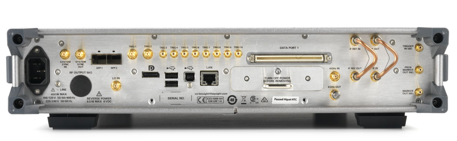
USB 2.0 master (2 ports) Allows control of USB devices. USB Type–A female connector. Nominal output current 0.5 A.
RF output Output impedance
50 Ω (nom).
– Option 520 or 52E Standard: Precision APC–3.5 male; plus
3.5 to 3.5 mm female adapter
Option 1ED: Type–N female; plus Type–N male to SMA female adapter
– Option 540 Precision APC–2.4 male; plus
2.4 to 2.4 mm and 2.4 to 2.92 mm female adapters
条件:Unless otherwise noted, digital outputs are 5 V CMOS, and digital inputs will accept 5 V CMOS, 3.3 V CMOS, or TTL voltage levels.
Option 1EM moves all connectors to the rear panel except the USB connectors.
hostname services, and TCP keep alive. This interface is LXI class C compliant.
USB 2.0 master (2 ports) Allows control of USB devices. USB Type–A female connector. Nominal output current 0.5 A.
USB 2.0 slave (1 port) Receives control from USB host. USB Type–B female connector. Nominal output current 0.5A.
LAN (1000BaseT) Allows LAN TCP/IP communication. RJ45 Ethertwist connector. The LAN connector provides SCPI
remote programming functionality. The LAN connector is used to access the internal web server and FTP
server. The LAN supports DHCP, HiSLIP, sockets SCIP, VXI–11 SCPI, connection monitoring, dynamic
SFP
1 Accepts an SFP+ transceiver
SFP
2 Accepts an SFP+ transceiver
DisplayPort Reserved for future use
Data Port 100–pin LVDS. This connector is used to provide agile LO control of the N519xA UXG agile signal
条件:6 GHz Out SMA; +10 dBm nominal output power.
Triggers 1 through 10 Triggers 1 – 2 are SMA; Triggers
3 – 10 are SMB.
High impedance inputs and 50 Ω outputs.
6 GHz In SMA; +5.0 dBm minimum input power. Damage level >
+15 dBm.
LO In SMA; +2.0 dBm minimum input power. Damage level >
+20 dBm.
条件:1. Please refer to the configuration guide for more details on configurations involving 2 vector UXGs.
Figure 14. Connections between the UXG agile vector adapter and the UXG agile signal generator 1, 2.
1. An alternative approach is to take the 6 GHz from the Analog UXG, split it, and take the output to each of the 6 GHz inputs of both the UXGs. Please reference
the configuration guide for more details. 2. For details on cables and accessories, please reference the configuration guide.
please contact your local Keysight office. The complete list is available at:
Trigger In 50 Ω SMB
Figure
13. The UXG agile vector adapter rear panel.
This information is subject to change without notice. © Keysight Technologies, 2017 - 2025, Published in USA, May 16, 2025
5992-2228EN
For more information on Keysight Technologies’ products, applications or services,
Publication title Publication number
N5194A and N5192A UXG Agile Vector Adapter – Configuration Guide
5992–2332EN
N5193A UXG Agile Signal Generator – Data Sheet
5992–0092EN
UXG Agile Signal Generator (N5193A and N5191A) – Configuration Guide
5992–1116EN
N5191A UXG X–Series Agile Signal Generator, Modified Version – Data Sheet
5992–1095EN
TAKE YOUR LAB TO THE NEXT LEVEL WITH Keysight Technologies Electronic Warfare
Test and Evaluation Solutions – Brochure
5992–3476EN
Solid state drive (SSD) capacity was increased from 480 GB to 512 GB on instruments with s/n ≥
5747xxxx, shipped after August
2017.
以上指标摘自厂家官方数据手册,完整定义、测试条件与保证值口径以手册为准。完整指标、测试条件与定义口径请见产品页「软件和手册 | 白皮书」栏目中的官方数据手册。
是德科技 | KEYSIGHT · onetest 仪器资源库


 客服











 粤公网安备44030902003758