是德科技 | KEYSIGHT
M9336A 任意波形发生器 540MHz 详细指标
Modular PXI Waveform and Function Generators
The warranted performance of a calibrated instrument that has been stored for a minimum of 1 hour
within the operating temperature range of 0 to 50 °C and after a
30-minute warm up period. All
specifications account for the effects of measurement and calibration-source uncertainties and were
created in compliance with ISO-17025 methods. In addition, a driver session must be opened to
initialize the power supplies. This can be done programmatically or by opening SFP and connecting to
the instrument. Data published in this document are specifications (spec) only where specifically
The characteristic performance, which 80% or more of manufactured instruments will meet. This data
is not warranted, does not include measurement uncertainty or calibration-source, and is valid only at
room temperature (approximately
25°C).
条件:and is measured at room temperature (approximately 25°C).
The mean or average characteristic performance, or the value of an attribute that is determined by
design such as a connector type, physical dimension, or operating speed. This data is not warranted
条件:such as amplitude drift vs. time. This data is not warranted and is measured at room temperature
An attribute measured during the design phase for purposes of communicating expected performance,
条件:performance within the operating temperature range unless otherwise noted. The data contained in
All data are measured from multiple units at room temperature and are representative of product
Bus interface and compatibility PXIe peripheral module (x8 Gen
2)
Module memory (option dependent)
2 or 4 GB
Maximum number of synchronized module s
8 (requires option PCH)
Supported waveform file formats M9336A binary format (.bin), CSV, Signal Studio (.wfm), and
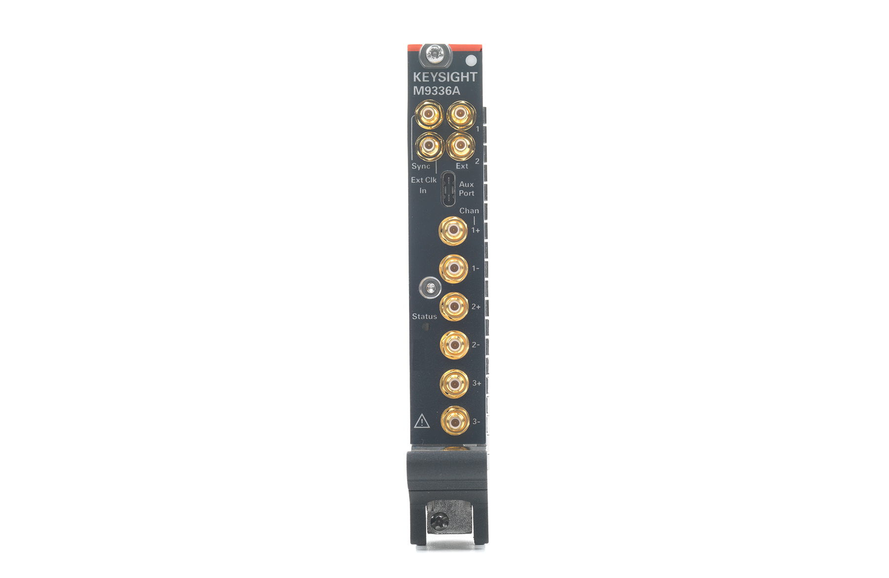
Ext1 and Ext2 SMB male
Channel
1+ and 1 - SMB male
Channel
2+ and 2 - SMB male
Channel
3+ and 3 - SMB male
Sync SMB male (enabled with M9336A-PCH option)
Size
3U/1-slot PXIe standard
130.1 x 21.7 x
210 mm; includes connectors and handle
Find us at www .keysight.com Page
11
Total power dissipated 48 W
54 W
Maximum channel bandwidth
540 MHz Option dependent
Maximum modulation (I/Q) bandwidth
1080 MHz Option dependent
Channel-to-channel alignment (meas)3
Between channels 1 and 2 <
20 ps
Between channels
3 and other
Between modules <
500 ps Requires option PCH
Delay range
±0.5 x (sample period) or ±1.6 µs
Delay resolution 0.1 ps for sample rates ≥
2.5 KSa/s
Delay resolution varies with sample rate below
2.5 KSa/s
Output Amplitude1
Amplitude resolution
16-bit (nom)
Amplitude DC accuracy (spec) ±0.5% of setting
±5 mV (spec)
Jitter2
Fc = 10 MHz <
1 ps rms (meas)
Fc ≥ 50 MHz <
0.25 ps rms (meas)
Rise/fall time (10% to 90%)
Without corrections <
1.2 ns, typical
With corrections <
900 ps, typical
1 Each output terminated with 50 ohms to ground.
2 1 kHz to 10 MHz integration bandwidth
3 Module-to-module alignment can be improved by usi ng an oscilloscope to manually characterize delays and compensate for
Find us at www .keysight.com Page
12
Single-ended Output Characteristics (nom)1
Characteristic Channels 1 & 2 Channel
3
50 Ω
Without corrections 0 Vpp to 1 Vpp
0 Vpp to 1.65 Vpp
With corrections 4 0 Vpp to 0.8 Vpp
0 Vpp to 1.26 Vpp
Range -0.3 to +0.81 V
±1.2 V
Adjustment resolution 100 uV
100 uV
Range 15 dB (min=0.11, max=0.66)
15 dB (min=0.18, max=1.08)
Adjustment resolution 0.0001
0.0001
Range min=0, max=1 min=0, max=1
Adjustment resolution 0.0001
0.0001
Differential Output Characteristics (nom)1
Characteristic Channels 1 & 2 Channel
3
Output impedance 100 Ω
100 Ω
Amplitude range2,3
Without corrections 0 Vpp to 2 Vpp
0 Vpp to 3.6 Vpp
With corrections 4 0 Vpp to 1.6 Vpp
0 Vpp to 2.5 Vpp
Adjustment resolution 100 uV
100 uV
Range -0.3 to +0.81 V
±1.20 V
Adjustment resolution 100 uV
100 uV
Range 15 dB (min=0.22, max=1.32)
15 dB (min=0.36, max=2.1)
Adjustment resolution 0.0001
0.0001
Range min=0, max=1 min=0, max=1
Adjustment resolution 0.0001
0.0001
1 Each output terminated with 50 ohms to ground.
2 With maximum analog and default digital gain sett ings. Higher levels of digital gain are possible depending on
signal type. For example, channels 1 and 2 can output a with a
1.3 Vpp sinewave. Using maximum digital gain on
complex waveforms with high crest factors may cause signal overload.
3 For channel 3, it is recommended to keep (Vpp X Frequency) < 2.5x10 8 and offsets =
0V to minimize harmonic
distortion. If offsets are used, it is recommended to keep (Vp X Frequency) <4x10
7
4 At maximum sample rate. Reducing sample rate will allow for higher amplitude settings.
Find us at www .keysight.com Page
13
条件:Figure 6. Nominal frequency response, channel 1-3
Ch 1 and Ch
2 corrected amplitude
flatness ±0.1 dB DC - 400 MHz ±0.15 dB
>400MHz - 540 MHz
Corrected phase flatness
±1 degree DC - 540 MHz
Analog reconstruction filter 540 MHz
9th order ellip tical, low pass
Find us at www .keysight.com Page
14
Spectral Characteristics (Channels
1 and 2)
Fc ≤ 200 MHz: 1 Vpp, 0.5 Voff (SE) or 2 Vpp, 0.8 Vcm ( Diff) ≤ -44 dBc ≤
-47 dBc
Fc ≤ 200 MHz: 1 Vpp, 0 Voff (SE) or 2 Vpp, 0 Vcm (Diff) ≤ -52 dBc ≤
-64 dBc
Fc ≤ 200 MHz: 0.5 Vpp, 0 Voff (SE) or 1 Vpp, 0 Vcm (Diff) ≤ -54 dBc ≤
-69 dBc
Fc ≤ 50 MHz: 1 Vpp, 0 Voff (SE) or 2 Vpp, 0 Vcm (Diff) ≤ -58 dBc ≤
-69 dBc
Fc = 500 MHz: 0.8 Vpp, 0 Voff (SE) or 1.6 Vpp, 0 Vcm (Diff) ≥ 37 dBc ≥
58 dBc Measured DC to 540 MHz
Fc = 200 MHz: 1 Vpp, 0 Voff (SE) or 2 Vpp, 0 Vcm (Diff) ≥ 58 dBc ≥
67 dBc Measured DC to 540 MHz
Fc = 50 MHz: 1 Vpp, 0 Vof f (SE) or 2 Vpp, 0 Vcm (Diff) ≥ 52 dBc ≥
67 dBc Measured DC to 135 MHz
Fc ≤ 200 MHz: 1 Vpp, 0.5 Voff (SE) or 2 Vpp, 0.8 Vcm (Diff) ≥ 44 dBc ≥
47 dBc Measured DC to 540 MHz
Fc ≤ 200 MHz: 1 Vpp, 0 Voff (SE) or 2 Vpp, 0 Vcm (Diff) ≥ 52 dBc ≥
63 dBc Measured DC to 540 MHz
Fc ≤ 200 MHz: 0.5 Vpp, 0 Voff (SE) or 1 Vpp, 0 Vcm (Diff) ≥ 53 dBc ≥
67 dBc Measured DC to 540 MHz
Fc ≤ 50 MHz: 1 Vpp, 0 Voff (SE) or 2 Vpp, 0 Vcm (Diff) ≥ 57 dBc ≥
67 dBc Measured DC to 135 MHz
Intermod distortion (I MD3)
Fc = 100 MHz ± 500 KHz: 1 Vpp, 0.5 Voff (SE) or 2 Vpp
0.8 Vcm
Fc = 100 MHz ± 500 KHz: 1 Vpp, 0 Voff (SE) or 2 Vpp, 0 Vcm (Diff) < -73 dBc <
-75 dBc
Fc = 10 MHz ± 500 KHz: 1 Vpp, 0.5 Voff (SE) or 2 Vpp, 0.8 Vcm (Diff) < -84 dBc <
-73 dBc
Fc = 10 MHz ± 500 KHz: 1 Vpp, 0 Voff (SE) or 2 Vpp, 0 Vcm (Diff) < -87 dBc <
-85 dBc
Third order intercept (TOI)
Fc = 100 MHz ± 500 KHz: 1 Vpp, 0.5 Voff (SE) or 2 Vpp
0.8 Vcm
Fc = 100 MHz ± 500 KHz: 1 Vpp , 0 Voff (SE) or 2 Vpp, 0 Vcm (Diff) > 35 dBm >
36 dBm
Fc = 10 MHz ± 500 KHz: 1 Vpp, 0.5 Voff (SE) or 2 Vpp, 0.8 Vcm (Diff) > 40 dBm >
35 dBm
Fc = 10 MHz ± 500 KHz: 1 Vpp, 0 Voff (SE) or 2 Vpp, 0 Vcm (Diff) > 42 dBm >
41 dBm
Output phase noise (100 M Hz output)
1 kHz offset -130 dBc/Hz
-130 dBc/Hz
10 kHz offset -135 dBc/Hz
-135 dBc/Hz
100 kHz offset -137 dBc/Hz
-137 dBc/Hz
1 MHz offset -152 dBc/Hz
-152 dBc/Hz
10 MHz offset -162 dBc/Hz
-162 dBc/Hz
≤ -159
条件:dBm/Hz 100 MHz tone, spot noise measured at 133 MHz
≤ -159
Figure 7. Typical Channel 1-2, 10 MHz tone spectrum Figure 8. Typical Channel 1-2
500 MHz tone spectrum
Find us at www .keysight.com Page
15
Spectral Characteristics (Channels
1 and 2) (cont’d)
Figure 9. Typical 2nd harmonic distortion, channel
1 and 2, single-ended
Figure 10. Typical 3rd harmonic distortion, channel
1 and 2, single-ended
Find us at www .keysight.com Page
16
Spectral Characteristics (Channels
1 and 2) (cont’d)
Figure 11. Typical 2nd harmonic distortion, channel
1 and 2, differential
Figure 12. Typical 3rd harmonic distortion, channel
1 and 2, differential
Find us at www .keysight.com Page
17
Spectral Characteristics (Channels
1 and 2) (cont’d)
Figure 13. Typical Channel 1-2, 100 MHz two tone Figure 14. Typical Channel
1-2 noise floor
Figure 15. Typical phase noise, channel
1 and 2
Find us at www .keysight.com Page
18
Spectral Characteristics (Channel
3) (cont’d)
Fc ≤ 200 MHz: 0.5 Vpp, 0.5 Voff (SE) or 1.0 Vpp, 0.5 Vcm (Diff) ≤ -31 dBc ≤
-38 dBc
Fc ≤ 200 MHz: 1.0 Vpp, 0 Voff (SE) or 2.0 Vpp, 0 Vcm (Diff) ≤ -41 dBc ≤
-47 dBc
Fc ≤ 200 MHz: 0.5 Vpp, 0 Voff (SE) or 1.0 Vpp, 0 Vcm (Diff) ≤ -48 dBc ≤
-60 dBc
Fc ≤ 50 MHz: 1.5 Vpp, 0 Voff (SE) or 3.0 Vpp, 0 Vcm (Diff) ≤ -66 dBc ≤
-64 dBc
Fc = 500 MHz: 0.25 Vpp, 0 Voff (SE) or 0.5 Vpp, 0 Vcm (Diff) ≥ 59 dBc ≥
54 dBc Measured DC to 540 MHz
Fc = 200 MHz: 0.5 Vpp, 0 Voff (SE) or 1.0 Vpp, 0 Vcm (Diff) ≥ 66 dBc ≥
71 dBc Measured DC to 540 MHz
Fc = 50 MHz: 1.5 Vpp, 0 Voff (SE) or 3.0 Vpp, 0 Vcm (\Diff) ≥ 64 dBc ≥
69 dBc Measured DC to 135 MHz
Fc ≤ 200 MHz: 0.5 Vpp, 0.5 Voff (SE) or 1.0 Vpp, 0.5 Vcm (Diff) ≥ 32 dBc ≥
39 dBc Measured DC to 540 MHz
Fc ≤ 200 MHz: 1.0 Vpp, 0 Voff (SE) or 2.0 Vpp, 0 Vcm (Diff) ≥ 41 dBc ≥
47 dBc Measured DC to 540 MHz
Fc ≤ 200 MHz: 0.5 Vpp, 0 Voff (SE) or 1.0 Vpp, 0 Vcm (Diff) ≥ 48 dBc ≥
58 dBc Measured DC to 540 MHz
Fc ≤ 50 MHz: 1.5 Vpp, 0 Voff (SE) or 3.0 Vpp, 0 Vcm (Diff) ≥ 60 dBc ≥
64 dBc Measured DC to 135 MHz
Intermod distortion (IMD3)
Fc = 100 MHz ± 500 KHz: 1.0 Vpp, 0.5 Voff (SE) or 2.0 Vpp
0.5 Vcm
Fc = 100 MHz ± 500 KHz: 1.0 Vpp, 0 Voff (SE) or 2.0 Vpp, 0 Vcm (Diff) < -71 dBc <
-72 dBc
Fc = 10 MHz ± 500 KHz: 1.0 Vpp, 0.5 Voff (SE) or 2.0 Vpp
0.5 Vcm
Fc = 10 MHz ± 500 KHz: 1.0 Vpp, 0 Voff (SE) or 2.0 Vpp, 0 Vcm (Diff) <
-79 dBc <-81 dBc
Third order intercept (TOI)
Fc = 100 MHz ± 500 KHz: 1.0 Vpp, 0.5 Voff (SE) or 2.0 Vpp
0.5 Vcm
Fc = 100 MHz ± 500 KHz: 1.0 Vpp, 0 Voff (SE) or 2.0 Vpp, 0 Vcm (Diff) > 34 dBm >
34 dBm
Fc = 10 MHz ± 500 KHz: 1.0 Vpp, 0.5 Voff (SE) or 2.0 Vpp
0.5 Vcm
Fc = 10 MHz ± 500 KHz: 1.0 Vpp, 0 Voff (SE) or 2.0 Vpp, 0 Vcm (Diff) > 38 dBm >
39 dBm
Output phase noise (100 MHz output)
1 kHz offset -130 dBc/Hz
-130 dBc/Hz
10 kHz offset -135 dBc/Hz
-135 dBc/Hz
100 kHz offset -137 dBc/Hz
-137 dBc/Hz
1 MHz offset -152 dBc/Hz
-152 dBc/Hz
10 MHz offset -162 dBc/Hz
-162 dBc/Hz
≤ -151
条件:dBm/Hz 100 MHz tone, spot noise measured at 133 MHz
≤ -151
Figure 16. Typical Channel 3, 10 MHz tone spectrum Figure 17. Typical Channel
500 MHz tone spectrum
Find us at www .keysight.com Page
19
Spectral Characteristics (Channel
3) (cont’d)
Figure 18. Typical 2nd harmonic distortion, channel
3, single-ended
Figure 19. Typical 3rd harmonic distortion, channel
3, single-ended
Find us at www .keysight.com Page
20
Spectral Characteristics (Channel
3) (cont’d)
Figure 20. Typical 2nd harmonic distortion, channel
3, differential
Figure 21. Typical 3rd harmonic distortion, channel
3, differential
Spectral Characteristics (Channel
3) (cont’d)
Figure 22. Typical Channel 3, 100 MHz two tone intermod Figure 23. Typical Channel
3 noise floor
Figure 24. Typical phase noise, channel
3
Find us at www .keysight.com Page
22
DAC sample rate
1.28 GSa/s
User sample rate (Fs) - option B12 1 Sa/s to 320 MSa/s
1µSa/s resolution
User sample rate (Fs) - option B50 1 Sa/s to 1.28 GSa/s
1µSa/s resolution
100 MHz Reference Clock
Clock sources PXIe_CLK100 and ExtClk In1
Clock lock range
±25 ppm (nom)
Ext Clk In Characteristics (nom)
1
Frequency Input 100 MHz
±25 ppm
Input level
100 mVPP to 5 VPP (square-wave or sine-wave)
Waveform memory (option dependent) Up to 500 MSa/ch
Waveform granularity (quantum)
4 samples
Maximum segments per sequence
227
Maximum number of sequences
225
条件:Maximum 2,145,300,000 samples (unlimited with option LW1)
Minimum - burst
12 samples
Minimum - looped
512 samples
Number of triggers
12 hardware and 12 software
Trigger sources Software, PXI_TRIG, PXI_STAR, DSTARB, Ext 1, Ext
2
Trigger polarity Positive or negative
Trigger timing resolution
3.125 ns
Minimum trigger width
20 ns
Trigger Jitter
±3.125 ns (typ)
Single module, correction filter off
322 ns + (24 x User sample period in ns)
Single module, correction filter on
2960 ns + (24 x User sample period in ns)
Multiple modules (opt PCH) 3.25 µs
± 50 ns
1 Supported on Serial Number MY5645030
9 and above
Find us at www .keysight.com Page
23
Maximum number of markers
8 per channel
Marker destinations PXI_TRIG, PXI_STAR, DSTARC, Ext1, and Ext2
Marker polarity Positive or negative
Marker placement accuracy
3.125 ns
Minimum trigger width
20 ns
Marker to waveform jitter Up to 3.125 ns, depending on waveform sample rate
Maximum number of markers Up to 3 depending on number of available channels
Marker destinations Analog output channels not being used for waveform
Marker type Precise data marker (timed precisely with waveform
Marker polarity Positive or negative
Marker to waveform jitter
25 ps
Marker on channels 1 and
20 ps
Range
±0.5 x (user sample period)
Resolution .001 ps
Marker width
4 user samples
Ext1 and Ext2 Characteristics (nom)
Direction Control Input or output (configurable)
Output impedance (output mode)
50 Ω
Maximum input level
±5.5 V
Input impedance (input mode)
10 kΩ
Minimum input swing
100 mV
Minimum input pulse width
10 ns
Programmable trigger input threshold
Programming resolution
10 mV
Find us at www .keysight.com Page
24
Modulation Format Specific Data
Typical EVM performance (meas)
1
802.11ax
EVM (80MHz, 1024 QAM)
0.2%
EVM (20MHz, 64 QAM)
0.075%
条件:Operating and Storage Condition s Operating Storage
Environmental Characteristics2,3
Temperature4 0˚C to 50˚C
-40˚C to 70˚C
Altitude Up to 10,000 ft (3048 m) Up to 15,000 ft (4572 m)
Humidity Type-tested at 95%
+40˚C (non-condensing)
Calibration interval
1 year
条件:EVM performance 2 Samples of this product have been type tested in accordance with the Keysight Environmental Test Manual and verified to be robust against the environ- mental stresses of Storage, Transportation and End-use; those stresses include but are not limited to temperature, humidity, shock, vibration, altitude and power line conditions.
Operating random vibration: type-tested at 5 to 500 Hz
0.21 g rms
Survival random vibration: type-tested at 5 to 500 Hz
2.09 g rms
1 With differential outputs and matched cables. Individual channel adjustments for gain and delay may be required to achieve be st
3 Test methods are aligned with IEC 60068-2 and levels are similar to MIL-PRF-28800F Class
3
4 De-rate max temperature by 5°C above
2000 m.
Find us at www .keysight.com Page
25
五、Regulatory Specifications
条件:versions of the following standards (dates and editions are cited in the Declaration of Conformity):
Complies with the essential requirements of the European Low Voltage Directive as well as the current
– Canada: CSA C22.2 No.
61010-1
条件:following standards (dates and editions are cited in the Declaration of Conformity):
Complies with the essential requirements of the European EMC Directive as well as the current editions of the
– CISPR Pub 11 Group
1, class A
– ICES/NMB-001
This ISM device complies with Canadian ICES
-001.
Cet appareil ISM est conformea la norme NMB-001 du Canada
This equipment has been conformity assessed for use in business environments. In a residential environment
条件:please contact your local Keysight office. The complete list is available at:
For more information on Keysight Technologies’ products, applications or services,
This information is subject to change without notice. © Keysight Technologies, 2020, Published in USA, February 24, 2020, 5992
-2140EN
Supported Software Components
Operating systems Microsoft Windows
7 and 10 (64-bit only)
Application development environments (ADE)
LabVIEW, MATLAB, Visual Studio.NET (C/C++, C#, VB.NET), Command Expert
Keysight IO libraries Version 2018 update
1 (or greater)
Playback on up to four modules per license)
• N76xxEMBC-1FP node-locked
• N76xxEMBC-1FL node-locked
12-month license
适用型号 N7602EMBC GSM/边沿/Evo
N7606EMBC Bluetooth (BR, EDR, LE
4.0
BT5)
N7608EMBC Custom
5G modulation
N7610EMBC IoT (Internet of Things)
802.11a/b/g/j/p/n/ac/ah/ax
N7624EMBC LTE/LTE-Advanced FDD
N7625EMBC LTE/LTE-Advanced TDD
M9336A PXIe I/Q arbitrary waveform generator: 500 MHz BW, 16-bit
3 scalar channels
M9336A-001 Enable I/Q channels (all
3 channels)
M9336A-B12 Channel Bandwidth
135 MHz
M9336A-B50 Channel Bandwidth
540 MHz
M9336A-LW1 Large waveform playback (up to 400 MHz I/Q)
M9336A-PCH Phase Coherent Operation
M9037A PXIe embedded controller: Intel i7, 4 GB RAM
240 GB SSD
M9010A PXIe chassis: 10-slot, 3U
24GB/s
M9018B PXIe chassis: 18-slot, 3U
8GB/s
M9019A PXIe chassis: 18-slot, 3U
24GB/s
以上指标摘自厂家官方数据手册,完整定义、测试条件与保证值口径以手册为准。完整指标、测试条件与定义口径请见产品页「软件和手册 | 白皮书」栏目中的官方数据手册。
是德科技 | KEYSIGHT · onetest 仪器资源库



 客服








 粤公网安备44030902003758