是德科技 | KEYSIGHT
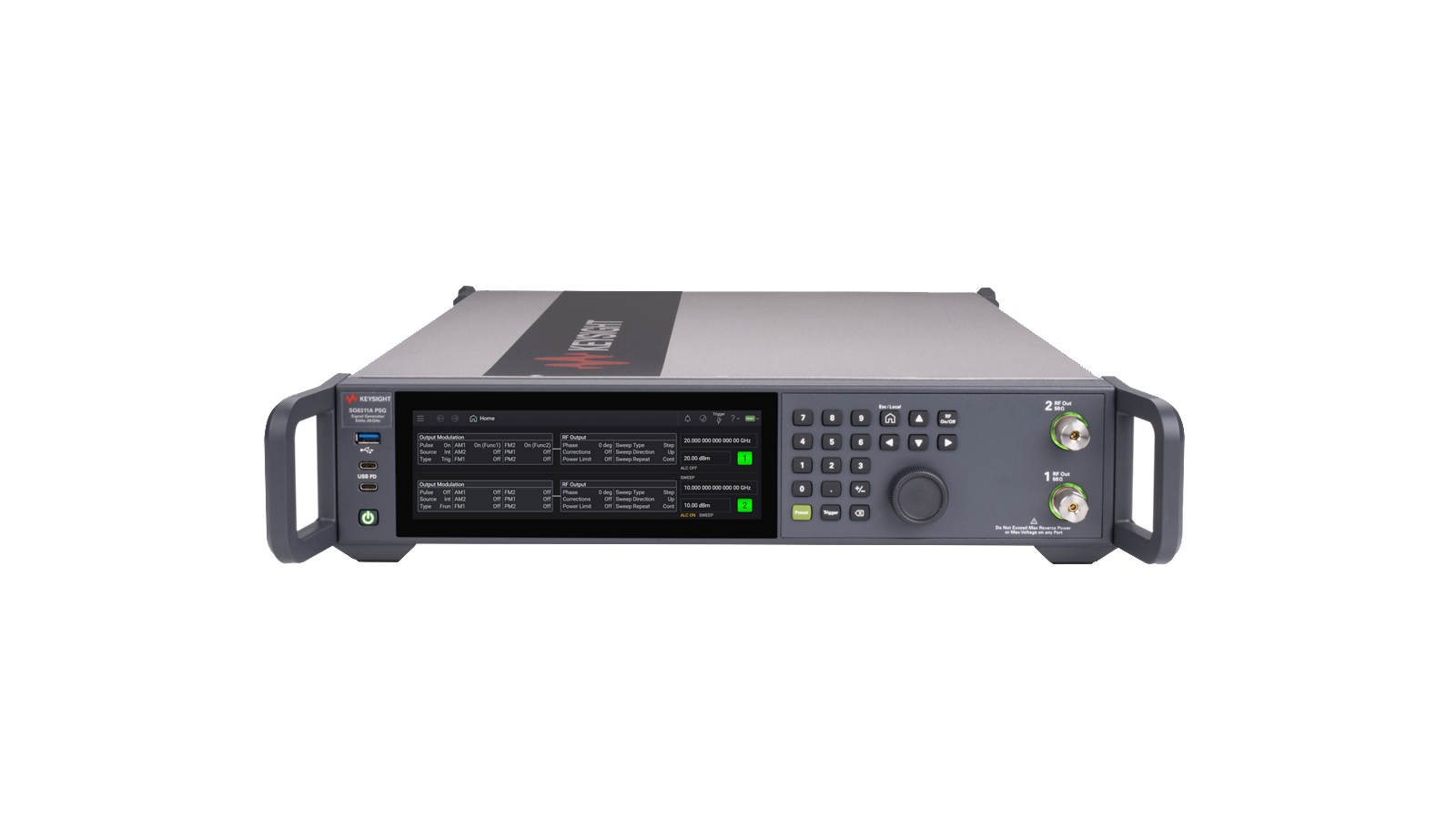
M9383A 14GHz至44GHz 信号发生器 19dBm 详细指标
Modular PXI Signal Sources
条件:Power search time < 20 ms, nominal
Maximum reverse power 1/2 Watt, 0 VDC, nominal
Output impedance
50 Ω, nominal
Operating modes Step Frequency start and stop (linear or logarithmic steps)
Step time Entry time
100 μs to 1 s
Number of points Step
1 to 3200
Input triggering Start step Immediate, external trigger, software trigger or software trigger button
End step Dwell time, entry time, external trigger, last segment, software trigger
Settled out Trigger when settled
< 50 MHz
-28 dBc (-30 dBc typ)
50 MHz to < 220 MHz
-31 dBc (-40 dBc typ)
220 MHz to < 2 GHz (Option 1EH filters Off)
-25 dBc (-30 dBc typ)
220 MHz to < 2 GHz (Option 1EH filters On)
-46 dBc (-48 dBc typ)
2 GHz to < 3.2 GHz
-55 dBc (-60 dBc typ)
3.2 GHz to < 3.4 GHz
-43 dBc (-45 dBc typ)
3.4 GHz to < 16 GHz
50 dBc (-55 dBc typ)
16 GHz to 22 GHz
-40 dBc (-52 dBc typ)
条件:Measured at 9 dBm or maximum specified power, whichever is lower. Sub-harmonics are defined as
Carrier Freq * (k/m), where k and m are integers, but excluding harmonics. Does not apply to non-
harmonic spurs which may overlap sub-harmonic spurs. Performance is unspecified for sub-harmonics
< 4.5 GHz
-55 dBc (-57 dBc typ)
4.5 GHz to < 5.2 GHz
-38 dBc (-47 dBc typ)
5.2 GHz to 20 GHz
-49 dBc (-55 dBc typ)
> 20 GHz to 44 GHz
-55 dBc (-57 dBc typ)
条件:Measured at 10 dBm or maximum specified power, whichever is lower. Non-harmonic spurs include
range. With option ST4, excludes 9.6 GHz and harmonics of 9.6 GHz with software earlier than 2.1.243.0.
mixing products for frequencies below
400 MHz, synthesizer spurs, and other miscellaneous chassis and
power supply products. Performance is unspecified for non-harmonics beyond the specified frequency
Fundamental frequency Sub-harmonic level 1 MHz to 20 GHz
-45 dBc (-55 dBc typ)
> 20 GHz to 44 GHz
-45 dBc (-50 dBc typ)
条件:Phase noise is measured with ALC off using a CW signal at +10 dBm or maximum specified power,
whichever is less. Phase noise specifications exclude external mechanical vibration.
Option ST2: Absolute SSB phase noise (dBc/Hz), spec (typ)
Offset from carrier 10 Hz 100 Hz 1 kHz 10 kHz 100 kHz 1 MHz 10 MHz 100 MHz
10 to 400 MHz (-75) (-95) (-110) (-117) (-116) (-136) (-137) (-135)
> 400 MHz to 10 GHz -40 (-51) -64 (-79) -91 (-97) -97 (-103) -97 (-102) -124 (-126) -128 (-141)
127 (-142)
> 10 GHz to 20 GHz -34 (-45) -60 (-73) -84 (-91) -92 (-97) -91 (-97) -117 (-125) -120 (-140)
-119 (-142)
> 20 GHz to 26.5 GHz (-38) (-68) ( -88) (
-95) (-94) (-119) (-136) (-147)
> 26.5 GHz to 44 GHz (-31) ( -59) ( -80) (
-84) (-85) (-114) (-124) (-125)
Option ST4: Absolute SSB phase noise (dBc/Hz), spec (typ)
Offset from carrier 10 Hz 100 Hz 1 kHz 10 kHz 100 kHz 1 MHz 10 MHz 100 MHz
10 to 400 MHz (-78) (-107) (-121) (-130) (-134) (-134) (-136) (-134)
> 400 MHz to 10 GHz -38 (-51) -65 (-80) -95 (-106) -109 (-118) -117 (-125) -119 (-123) -133 (-142)
-133 (-143)
> 10 GHz to 20 GHz -30 (-44) -58 (-74) -87 (-100) -101 (-113) -111 (-119) -113 (-119) -125 (-139)
-123 (-141)
> 20 GHz to 26.5 GHz (-41) (-70) (-98) (-110) (-117) (-117) (-134) (-141)
> 26.5 GHz to 44 GHz (-23) (-53) (-84) (-102) (-110) (-110) (-125) (-125)
条件:Frequency switching speed (nominal) 1
1. Measured at 0 dBm in step mode with ALC off from a trigger until frequency is settled within 1 ppm or 100 Hz of final value,
whichever is greater, and amplitude is settled within 0.2 dB of final value.
Specifications apply with attenuator hold off (default mode) and output level ≤ 10 dBm from 20 to 30 °C.
Frequency Standard Option UNQ Option UNZ 400 MHz to < 3.2 GHz 16 ms 300 μs 300 μs 3.2 GHz to < 10 GHz 16 ms 7 ms 7 ms 10 GHz to < 20 GHz 16 ms 7 ms
7 ms
20 GHz to < 31.8 GHz 6 ms 250 μs
250 μs
31.8 GHz to 37 GHz 6 ms 750 μs
250 μs
> 37 GHz to 44 GHz 6 ms 250 μs
250 μs
Pulse Modulation (Option PM1 or PM2)
Mode Option PM1 Option PM2
ALC off, 10 MHz to 20 GHz 100 ns
100 ns
ALC off, > 20 GHz 30 ns
20 ns
On/Off ratio without I/Q modulation Frequency Option F14 or F20 Option F32 or F44
10 MHz to 10 GHz 70 dB
70 dB
> 10 GHz to 20 GHz 60 dB (typ)
60 dB (typ)
> 20 GHz to 44 GHz n/a
80 dB
On/Off ratio with I/Q burst aligned to pulse (Option B04, B05, B16, B17,
适用型号 C05, C06, C10 或 C11)
条件:1. For pulse width ≥ 1 us with ALC on and for pulse width ≥ 50 ns with ALC off after power search.
2. With step attenuator in 0 dB position. Video feed -through decreases directly with step attenuator setting.
= 50 ns, pulse period = 200 ns. The oscilloscope is protected by a 10 dB pad and the timescale is set to 10 ns/div.
Frequency Option F14 or F20 Option F32 or F44
10 MHz to 10 GHz 80 dB (nom)
80 dB (nom)
> 10 GHz to 20 GHz 80 dB (nom)
80 dB (nom)
> 20 GHz to 44 GHz n/a
80 dB (nom)
Rise/fall times (Tr and Tf) ALC off
10 ns (typ)
Level accuracy (relative to CW) 1 10 MHz to 30 GHz
± 1 dB (typ)
> 30 GHz
± 1.5 dB (typ)
Width accuracy RF width relative to setting
± 16 ns
Width compression (Trf-Tw) RF width relative to video out
± 19 ns (meas)
Video feed-through (Vf) 2 0.4 GHz to 3.2 GHz <
200 mV pk-pk (typ)
> 3.2 GHz to 5.2 GHz <
100 mV pk-pk (typ)
> 5.2 GHz to 44 GHz <
30 mV pk-pk (typ)
Pulse overshoot ≤ 3.2 GHz <
15% (typ)
> 3.2 GHz <
5% (typ)
External input level
+1 V = RF on
0 V = RF off
External input impedance
50 Ω (nom)
Figure 3. Measured pulse shape; Frequency = 9 GHz, power = 5 dBm, amplitude =
5 dBm, ALC off, pulse width
Internal pulse generator (Option PM1 or PM2)
Triggering Free run, triggered, gated, and external pulse
Triggers Trig 1, Trig 2, Backplane
0-7
Signal routing Sync to Sync, Trig/Pulse in to TRIG1, video out to TRIG2
Square wave rate (50 MHz)/k from 0.1 Hz to 50 MHz where k is an integer (nom)
Option PM1 Option PM2
Pulse period (PRI) (Tp) 30 ns to 41.99 s
20 ns to 41.99 s
Pulse width (Tw) 30 ns to 41.99 s
20 ns to 41.99 s
Video delay (Td) Free run ± 4 μs
± 4 μs
Triggered modes 0 to 42 s
0 to 42 s
RF delay (Tm) 0 to 42 s
0 to 42 s
Sync trigger 30 ns to 3.99 μs
20 ns to 3.99 μs
Pulse doublets Delay 1 0 to 42 s
0 to 42 s
Pulse width 1 30 ns to 60 ns
20 ns to 60 ns
Delay 2 60 ns to 42 s
60 ns to 42 s
Pulse width 2 30 ns to 42 s
20 ns to 42 s
Pulse train Repetitions 1 to 2046
1 to 2046
On time 30 ns to 42 s
20 ns to 42 s
Off time 30 ns to 42 s
20 ns to 42 s
条件:Refer to the N value in the table of frequency bands. With Option ST4 and FM on, the effective phase
noise and spectral purity are equivalent to Option ST2. Using FM through the ”ARB Modulation”
条件:Maximum peak deviation ± N × 10 MHz, nominal
Deviation resolution
0.1% of deviation or 1 Hz, whichever is greater
条件:Deviation accuracy Measured at a 1 kHz rate with deviation
Distortion Measured at a 1 kHz rate with deviation
≤ 100 kHz, freq ≤ 20 GHz
20 to 30 °C
±(3.5% of deviation +
20 Hz)
< 3.5% (typ)
Modulation frequency response
1
Mode 1 dB bandwidth
3 dB bandwidth
DC coupling DC to 100 kHz (nom) DC to 10 MHz (nom)
AC coupling 5 Hz to 100 kHz (nom)
5 Hz to 10 MHz (nom)
External DC FM carrier offset 2 ± (0.2% of set deviation + N x
8 Hz) (typ)
External input sensitivity
± 1 Vpeak for indicated deviation
± 1.2 V max
External input impedance 50 Ω
600 Ω or 1 MΩ, selectable (nom)
适用型号频率调制 (选件 B04, B05, B16, B17, C05, C06, C10 或 C11)
条件:Modulation subsystem provides wider bandwidths but does not provide external inputs.
This section describes frequency modulation through the “ARB Modulation” subsystem. For frequency
modulation through the synthesizer subsystem, see “Frequency modulation (Option UNT)”. The ARB
Option Frequency < 3.2 GHz Frequency ≥
3.2 GHz
B04 or B05 0 Hz to 12.5 MHz
0 Hz to 12.5 MHz
B16 or B17 0 Hz to 50 MHz
0 Hz to 50 MHz
C05 or C06 0 Hz to 50 MHz
0 Hz to 160 MHz
C10 or C11 0 Hz to 50 MHz
0 Hz to 320 MHz
Option Frequency < 3.2 GHz Frequency ≥
3.2 GHz
B04 or B05 1 Hz to 12.5 MHz
1 Hz to 12.5 MHz
B16 or B17 1 Hz to 50 MHz
1 Hz to 50 MHz
C05 or C06 1 Hz to 50 MHz
1 Hz to 160 MHz
C10 or C11 1 Hz to 50 MHz
1 Hz to 320 MHz
Waveforms Sine, dual-sine, triangle, ramp up, ramp down, square
条件:Refer to the N value in the table of frequency bands. With Option ST4 and phase modulation on, the
effective phase noise and spectral purity are equivalent to Option ST2. Using phase modulation through
the “ARB Modulation” subsystem does not have this limitation.
Maximum peak deviation ± N ×
2 rad (nom)
Deviation resolution
0.1% of set deviation (nom)
条件:Measured at a 1 kHz rate, freq ≤ 20 GHz,
20 to 30 °C, deviation >=
0.2 rad
±(5% of deviation +
0.01 rad)
Distortion
1 Total harmonic distortion
Modulation frequency response
2
DC coupling DC to 100 kHz (nom) DC to 1 MHz (nom)
AC coupling 5 Hz to 100 kHz (nom)
5 Hz to 1 MHz (nom)
External input sensitivity
± 1 Vpeak for indicated deviation
± 1.2 V max
External input impedance 50 Ω
600 Ω or 1 MΩ, selectable (nom)
适用型号相位调制 (选件 B04, B05, B16, B17, C05, C06, C10 或 C11)
条件:Modulation subsystem provides wider bandwidths but does not provide external inputs.
This section describes phase modulation through the ”ARB Modulation” subsystem. For phase
modulation through the synthesizer subsystem, see ”Phase modulation (Option UNT)”. The ARB
Option Frequency < 3.2 GHz Frequency ≥
3.2 GHz
B04 or B05 1 Hz to 12.5 MHz
1 Hz to 12.5 MHz
B16 or B17 1 Hz to 50 MHz
1 Hz to 50 MHz
C05 or C06 1 Hz to 50 MHz
1 Hz to 160 MHz
C10 or C11 1 Hz to 50 MHz
1 Hz to 320 MHz
Peak deviation
0 to 10 rad (nom)
Waveforms Sine, dual-sine, triangle, ramp up, ramp down, square
条件:maximum specified power. With ALC Off, specifications apply after power search is executed.
AM performance is not specified with attenuator hold on, above
20 GHz or when AM peaks exceed
Linear mode Exponential (log) mode
Depth Maximum (ALC off) 99%
40 dB
Settable range 0 to 100%
0 to 40 dB
Depth accuracy ALC on
1 kHz rate, depth ≤
External input Polarity Selectable Downward modulation only
Sensitivity for indicated depth ± 1 V (nom)
-1 V (nom)
Maximum voltage range ± 1.2 V (nom)
-1.2 V to 0 V (nom)
Modulation frequency response
1
DC coupling DC to 70 kHz (nom)
AC coupling
5 Hz to 70 kHz (nom)
Distortion 30% AM, 1 kHz rate <
2.0% total harmonic distortion (typ)
60% AM, 1 kHz rate <
2.5% total harmonic distortion (typ)
External Input Impedance 50 Ω
600 Ω or 1 MΩ
适用型号幅度调制 (选件 B04, B05, B16, B17, C05, C06, C10 或 C11)
条件:specified power. With ALC Off, specifications apply after power search is executed.
This section describes amplitude modulation through the “ARB Modulation” subsystem. For amplitude
modulation through the output subsystem, see “Amplitude modulation (Option UNT)”. The ARB
Modulation subsystem provides better amplitude accuracy but does not provide external inputs. AM
performance is not specified with attenuator hold on, above
20 GHz or when AM peaks exceed maximum
Option Frequency < 3.2 GHz Frequency ≥
3.2 GHz
B04 or B05 1 Hz to 25 MHz
1 Hz to 25 MHz
B16 or B17 1 Hz to 100 MHz
1 Hz to 100 MHz
C05 or C06 1 Hz to 100 MHz
1 Hz to 320 MHz
C10 or C11 1 Hz to 100 MHz
1 Hz to 640 MHz
Waveforms Sine, dual-sine, triangle, ramp up, ramp down, square
条件:AM function generator Provides one signal for use with AM or M9312A LF output.
FM function generator Provides one signal for use with FM, ΦM or M9303A LF output.
Output Internal 1, internal 2, noise generator 1, noise generator
2
Monitoring Provides monitoring of function generators when used for AM, FM, or ΦM
Output impedance
50 Ω (nom)
Types Sine, pulse, positive ramp, negative ramp, triangle, noise, dual sine, dual
Rate range Sine
0.1 Hz to 10 MHz
Other waveforms
0.1 Hz to 1 MHz
Rate resolution
0.1 Hz Rate resolution
速率精度 Same as PXIe backplane reference 速率精度
Phase offset
-6.29 rad to +6.29 rad Phase offset
Pulse duty cycle
0% to 100% Pulse duty cycle
适用型号 C05, C06, C10 或 C11)
External I/Q inputs (Option
016)
Type Differential: I, I̅, Q, Q̅
条件:modulator attenuator which may be either manually or automatically set.
Input impedance
50 Ω (nom)
Recommended input level -1 dBm or √I2 + Q2 =
0.2 Vrms (nom)
Input level range Different RMS levels are accommodated by adjusting the internal I/Q
The minimum input level required to maintain RF level accuracy is
√I2 + Q2 = 0.1 Vrms. Minimum 0.1 Vrms, maximum
1 Vpeak
External I/Q bandwidth (Option
016)
< 3.2 GHz DC to 80 MHz (nom)
160 MHz (nom)
≥ 3.2 GHz DC to 1 GHz (nom)
2 GHz (nom)
条件:I/Q input adjustments (Option 016 with Option C05, C06, C10 or C11)
I and Q offset adjustment
± 50% (nom)
I/Q quadrature skew adjustment <
3.2 GHz none
I/Q gain balance adjustment
± 10 dB (nom)
Delay adjustment Option B04 or B05
± 125 ns (nom)
Option B16 or B17
± 250 ns (nom)
Option C05 or C06
± 19 ns (nom)
Option C10 or C11
± 39.1 ns (nom)
Type Differential: I, I̅, Q, Q̅
条件:1. All output voltages measured with a 50 Ω load.
Frequency range DC to 80 MHz (nom) for 1 dB bandwidth
DC offset adjustments
± 3 V
Common-mode I/Q offset
± 200 mV (nom)
Differential mode I or Q offset
± 50 mV (nom)
I/Q baseband output amplitude
1
Internal I/Q modulation
0.8 Vrms (typ)
External I/Q modulation Variable from 0.8 to 1.8 Vrms (typ)
Internal Baseband Generator (Option B04, B05,
In-phase and Quadrature (I and Q) and a third channel (3)
Resolution
16 bits [1/65536]
Option Frequency < 3.2 GHz Frequency ≥
3.2 GHz
B16 or B17 160 MHz
160 MHz
C05 or C06 160 MHz
500 MHz
Option Frequency < 3.2 GHz Frequency ≥
3.2 GHz
B04 or B05 50 MSa/s
50 MSa/s
B16 or B17 200 MSa/s
200 MSa/s
C05 or C06 200 MSa/s
625 MSa/s
C10 or C11 200 MSa/s
1.28 GSa/s
Frequency offset range (Option B04, B05, B16 or B17)
B04 or B05
-20 MHz to +20 MHz
B16 or B17
-80 MHz to +80 MHz
Real-time additive noise impairment (AWGN) (Option B04, B05, B16 or B17)
Type Real-time, continuously calculated, and played using DSP
Carrier-to-noise ratio
0 dBc to 70 dBc
Bandwidth Option B04 or B05
1 Hz to 40 MHz
Option B16 or B17
1 Hz to 160 MHz
Internal baseband generator
Real-time phase noise impairment (Option B04, B05, B16 or B17)
Close-in phase noise characteristics
-20 dB per decade
Far-out phase noise characteristics
-20 dB per decade
Start frequency (f1) Offset settable from 0 to 20 MHz
Stop frequency (f2) Offset settable from 0 to 20 MHz
User selected; max degradation dependent on f2
Play start trigger Immediate, external, software trigger, software trigger button
ALC hold trigger None, Marker 1, Marker 2, Marker 3, Marker
4
Pulse trigger None, Marker 1, Marker 2, Marker 3, Marker
4
None, Per waveform, Marker 1, Marker 2, Marker 3, Marker
4
None, Marker 1, Marker 2, Marker 3, Marker
4
Markers can be routed to the ALC hold function and the pulse modulator
Marker polarity Negative, positive
条件:1. Number of tones at selected spacing cannot exceed RF bandwidth .
Option B04 or B05
100 Hz to 50 MHz
Option B16 or B17
100 Hz to 100 MHz
Option C05 or C06
100 Hz to 320 MHz
Option C10 or C11
100 Hz to 640 MHz
Auxiliary waveform generator (Option C05, C06, C10 or C11)
Auxiliary waveform generator
Channel name
3+ and 3- (Aux Awg)
Option Frequency < 3.2 GHz Frequency ≥
3.2 GHz
B04 or B05 50 MSa/s
50 MSa/s
B16 or B17 200 MSa/s
200 MSa/s
C05 or C06 200 MSa/s
625 MSa/s
C10 or C11 200 MSa/s
1.28 GSa/s
Modes Free run, synchronous with I/Q channels
Load impedance
48.5 to 51.5 Ω
Software drivers IVI.NET, IVI-COM, IVI-C
条件:Interfaces GPIB (IEEE-488.2,1987) with listen and talk, and 1000BaseT LAN interface.
Control languages SCPI version
1997.0.
IEEE-488 functions SH1, AH1, T6, TE0, L4, LE0, SR1, RL1, PP0, DC1, DT0, C0, E2
Keysight IO libraries Keysight’s IO Library Suite helps you quickly establish an error-free connection between
your PC and instruments - regardless of the vendor. It provides robust instrument control
and works with the software development environment you choose.
Non-operating (storage)
0 to 50 °C
−40 to +70 °C
Humidity 1 Type tested at 95%
+40 °C (non-condensing)
条件:temperature, humidity, shock, vibration, altitude and power-line conditions. Test methods
Type tested at 5 to 500 Hz
0.21 g rms
Type tested at 5 to 500 Hz
2.09 g rms
Type tested at half-sine, 30 g
11 ms Type
tested per MIL-PRF-28800F
Altitude Up to 15,000 feet (4,572 meters)
2
EMC Complies with European EMC Directive
2004/108/EC
• CISPR Pub 11 Group
1, class A
• ICES/NMB-001
This ISM device complies with Canadian ICES-001.
Cet appareil ISM est conforme a la norme NMB-001 du Canada.
Environmental testing Samples of this product have been type tested in accordance with the Keysight
Environmental Test Manual and verified to be robust against the environmental stresses
of storage, transportation and end-use. Those stresses include but are not limited to
are aligned with IEC 60068-2 and levels are similar to MIL-PRF-28800F Class
3. Phase
noise specifications are not warranted in a vibrating environment.
ISO compliant This family of signal generators is manufactured in an ISO-9001 registered facility in
concurrence with Keysight’s commitment to quality
条件:Self-test Internal diagnostic routine tests most modules in a preset condition. If a module’s node
voltages are within acceptable limits, then the module passes the test.
1. Samples of this product have been type tested in accordance with the Keysight Environmental Test Manual and verified to be
to temp erature, humidity, shock, vibration, altitude and power -line conditions. Test methods are aligned with IEC 60068 -2 and
2. At 15,000 feet, the maximum environmental temperature is de -rated to 40 °C.
robust against the environmental stresses of storage, transportation and end -use — those stresses include but are not limited
levels are similar to MIL -PRF -28800F Class
3.
模块尺寸 Length Width Height 重量重量
M9300A 1 PXIe slot 210 mm 22 mm 130 mm 0.55 kg
1.22 lbs
M9303A 1 PXIe slot 210 mm 22 mm 130 mm 0.57 kg
1.25 lbs
M9305A 2 PXIe slots 210 mm 42 mm 130 mm 0.91 kg
2.00 lbs
M9312A 3 PXIe slots 210 mm 62 mm 130 mm 1.86 kg
4.10 lbs
M9314A 2 PXIe slots 210 mm 42 mm 130 mm 1.21 kg
2.67 lbs
M9316A 3 PXIe slots 210 mm 62 mm 130 mm 1.70 kg
3.75 lbs
M9318A 3 PXIe slots 210 mm 62 mm 130 mm 1.70 kg
3.75 lbs
M9405A 1 PXIe slot 210 mm 22 mm 130 mm 0.57 kg
1.25 lbs
M9155CH40 1 PXIe slot 210 mm 22 mm 130 mm 0.40 kg
0.88 lbs
Module 5 V 5 V VIO 12 V 3.3 V -12 V
5 V Aux Total
M9300A 0 W 0 W 17 W 2 W 0 W 0 W
19 W
M9303A 0 W 0 W 38 W 10 W 0 W 0 W
48 W
M9305A 0 W 0 W 21 W 5 W 0 W 0 W
26 W
M9312A 0 W 0 W 82 W 2 W 0 W 0 W
84 W
M9314A 0 W 0 W 44 W 2 W 0 W 0 W
46 W
M9316A 0 W 0 W 64 W 15 W 0 W 0 W
79 W
M9318A 0 W 0 W 95 W 15 W 0 W 0 W
110 W
M9405A 0 W 0 W 3 W 0 W 0 W 0 W
3 W
M9155CH40 0.1 W 0 W 5 W 2 W 0 W 0 W
7.1 W
Operating systems Windows 7 (32-bit and 64-bit), Windows
10 (32-bit and 64-bit)
Processor speed 1 GHz 32-bit (x86), 1 GHz 64-bit (x64) (no support for Itanium
64)
Available memory
4 GB minimum
8 GB or greater recommended
Available disk space
1.5 GB available hard disk space
Video Support for DirectX
9 graphics with 128 MB graphics memory recommended (Super
VGA graphics is supported)
Browser Microsoft Internet Explorer
7 or greater
Keysight IO libraries Version
16.3.17914 or later
条件:RF Out SMA (f) connector. Outputs the primary RF signal of the synthesizer. Nominal frequency
range is 187.5 MHz to 13.7 GHz. Nominal power range is 0 to 15 dBm from 187.5 MHz to
10 GHz and 0 to 10 dBm from 10 GHz to 13.7 GHz. 50 Ω nominal impedance.
RF In SMA (f) connector. Accepts an RF signal which can be routed to RF Out. Nominal
frequency range is 10 MHz to 6 GHz. Nominal power is 5 dBm. 50 Ω nominal impedance.
FM In SMP (m) connector. Drives either FM or M , selectable. Nominal frequency range is DC
M . Nominal impedance is 50 Ω, 600 Ω, and 1MΩ, selectable. Damage level is ±5 V.
clock input. Nominal power is 10 dBm. 50 Ω nominal impedance. Damage level is 20 dBm.
clock input. Output can be switched on or off. Nominal power is 10 dBm. 50 Ω nominal
clock input. Nominal power is 10 dBm. 50 Ω nominal impedance. Damage level is 20 dBm.
Nominal power is 13 dBm. 50 Ω nominal impedance.
multiple modules. Nominal power is 12 dBm. 50 Ω nominal impedance.
the FM modulation. Nominal frequency range is DC to 10 MHz. Nominal voltage is 0 to 5 V
peak into 50 Ω with a -5 V to 5 V offset. 50 Ω nominal impedance.
input, trigger level is adjustable from -2.1 V to +4.1 V. 50 Ω nominal impedance.
input, trigger level is adjustable from -2.1 V to +4.1 V. 50 Ω nominal impedance. Damage
nominal impedance. Damage level is ± 5 V.
Status LED indicator. Green = functioning properly. Red = fault condition.
RF Out SMA (f) connector. Provides the RF Output. Nominal frequency range is 150 MHz to
1.2 GHz. Nominal power is 5 dBm. 50 Ω nominal impedance. Damage level is 17 dBm.
DDS In SMA (f) connector. Accepts the DDS signal for use by the module. Nominal frequency range is
150 MHz to 1.2 GHz. Nominal power is -5 dBm. 50 Ω nominal impedance. Damage level is
DDS Out SMA (f) connector. Outputs a copy of the signal from DDS In. Nominal frequency range is 150 MHz
to 1.2 GHz. Nominal power is 5 dBm. 50 Ω nominal impedance. Damage level is 17 dBm.
4.8 GHz In SMA (f) connector. Accepts a 4.8 GHz reference clock. Nominal power is 10 dBm. 50 Ω nominal
Nominal power is 10 dBm. 50 Ω nominal impedance. Damage level is 14 dBm.
Clock In SMA (f) connector. Accepts a clock for use by the DDS system. Nominal frequency is
4.8 GHz. Nominal power is 10 dBm. 50 Ω nominal impedance. Damage level is 17 dBm.
Clock Out SMA (f) connector. Provides a copy of the signal from Clock In. Nominal frequency is
4.8 GHz. Nominal power is 10 dBm. 50 Ω nominal impedance. Damage level is 14 dBm.
Trig 1 SMP (m) connector. Bidirectional signal for trigger and events. 1 MΩ nominal impedance. Damage
Trig 2 SMP (m) connector. Bidirectional signal for trigger and events. 1 MΩ nominal impedance. Damage
Sync SMP (m) connector. Bidirectional signal for synchronization with other modules. 1 MΩ nominal
Status LED indicator. Green = functioning properly. Blue = software not connected. Red = fault condition.
USB connector Unlabeled. Reserved for future use. Not for use with USB devices.
RF 1 In SMA (f) connector. Accepts a 3.2 to 20 GHz IF signal. 50 Ω nominal impedance.
RF 2 In SMA (f) connector. Accepts a 400 MHz to 3.2 GHz IF signal. 50 Ω nominal impedance.
are connected by a jumper. 50 Ω nominal impedance.
Aux Out SMA (f) connector. Provides the output signal before the output attenuator. 50 Ω nominal
The connection diagram is found in the M9383A Startup Guide, M9383-90001
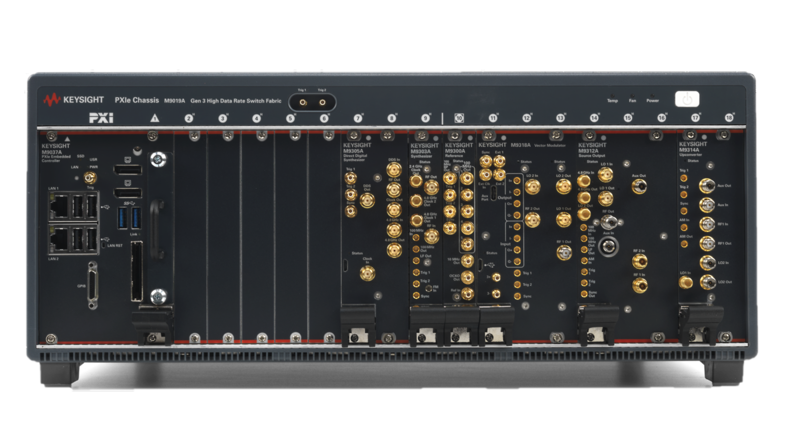
M9300A PXIe frequency reference - 1 slot
See the M9300A datasheet (5991-0898EN) for the table of input and output connectors
M9303A PXIe synthesizer - 1 slot
to 10 MHz for FM and DC to 1 MHz for
2.4 GHz Clock Out APC 3.5 mm (f) connector. Outputs the internal 2.4 GHz clock derived from the
100 MHz
4.8 GHz Clock 2 Out APC 3.5 mm (f) connector. Outputs the internal 4.8 GHz clock derived from the
100 MHz
impedance. Damage level is
20 dBm.
4.8 GHz Clock 1 Out APC 3.5 mm (f) connector. Outputs the internal 4.8 GHz clock derived from the
100 MHz
100 MHz In SMP (m) connector. Accepts a
100 MHz clock input as a timebase for the synthesizer.
100 MHz Out SMP (m) connector. Outputs a copy of the
100 MHz clock input for use in a daisy chain of
LF out SMP (m) connector. Outputs the waveform from the internal function generator or a copy of
Trig 1 SMP (m) connector. Bidirectional signal for trigger and events. When configured as an
output, VOL < 0.4 V, VOH is
2.8 V to 3.3 V into high impedance. When configured as an
Trig 2 SMP (m) connector. Bidirectional signal for trigger and events. When configured as an
output, VOL < 0.4 V, VOH is
2.8 V to 3.3 V into high impedance. When configured as an
Sync SMP (m) connector. Bidirectional signal for synchronization with other modules.
50 Ω
M9305A PXIe digital direct synthesizer - 2 slots
17 dBm.
impedance. Damage level is
25 dBm.
4.8 GHz Out SMA (f) connector. Outputs a copy of the signal from 4.8 GHz In. Output can be switched on or off.
level is 10 Vpeak
5 V rms.
level is 10 Vpeak
5 V rms.
impedance. Damage level is 10 Vpeak
5 V rms.
M9312A PXIe source output - 3 slots
Aux In SMA (f) connector. Accepts an output signal from 1 MHz to 44 GHz. Normally Aux Out and Aux In
以上指标摘自厂家官方数据手册,完整定义、测试条件与保证值口径以手册为准。完整指标、测试条件与定义口径请见产品页「软件和手册 | 白皮书」栏目中的官方数据手册。
是德科技 | KEYSIGHT · onetest 仪器资源库


 客服








 粤公网安备44030902003758