

 客服




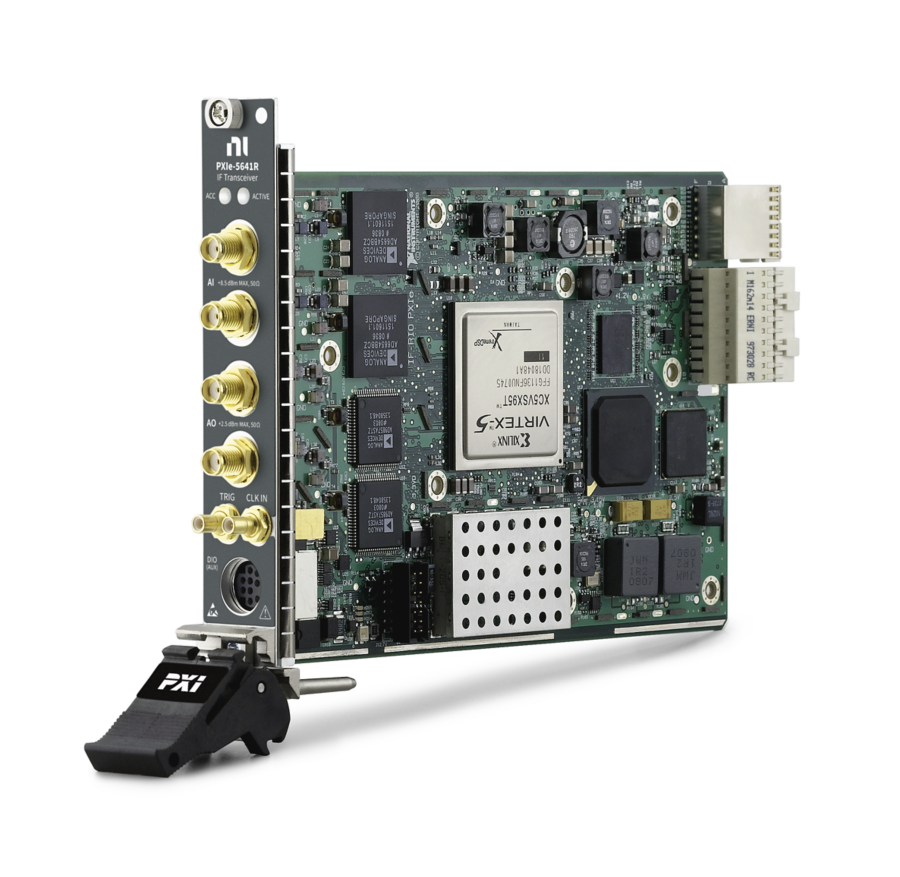
输入通道数量:2
输出通道数量:2
RF频率范围:0 MHz 至 80 MHz
最大输出功率:2 dBm
双输入/双输出PXI IF收发仪
ONETEST 欢迎您
厂商登录 | 入驻
登录 | 注册 购物车 微信公众号厂商登录
输入通道数量:2
输出通道数量:2
RF频率范围:0 MHz 至 80 MHz
最大输出功率:2 dBm
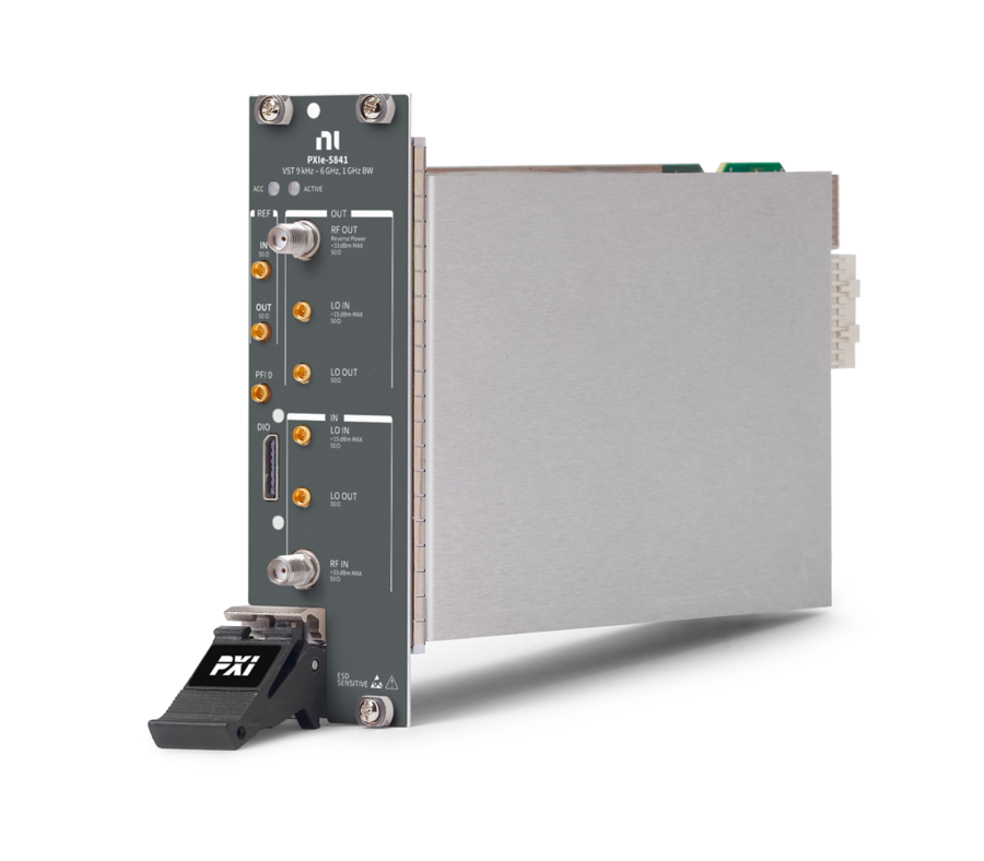
双输入/双输出PXI IF收发仪
以下指标取自 Teledyne 官方在线规格书,按原文档小节分组。
| 1 | +5 V |
| 2 | Digital ground (DGND) |
| 3 | DIO_01 |
| 4 | DIO_02 |
| 5 | DIO_03 |
| 6 | DIO_04 |
| 7 | DIO_05 |
| 8 | DIO_06 |
| 9 | DIO_07 |
| Number of channels | 2 |
| ADC resolution | 14 bits |
| Sample rate | 30 MS/s to 100 MS/s |
| Full-scale input range | +8.5 dBm peak at 10 MHz ± 1 dB typical (1.7 Vpeak–peak sine, 0.60 VRMS) |
| Maximum input level without damage | +24 dBm peak (10Vpeak–peak sine, 3.5 VRMS) |
| Input coupling | AC |
| Input impedance | 50 Ω nominal |
| Input return loss | <-15 dB typical, 250 kHz to 80 MHz |
| Maximum DC input voltage without damage | 10 V |
| Average noise density | -143 dBm/Hz typical |
| Signal-to-noise ratio | >76 dB typical (-1 dBfs at 68 MHz tone, bandwidth = 10 MHz) |
| Maximum instantaneous bandwidth | 20 MHz (limited by digital downconverter) |
| Passband flatness (referenced to 10 MHz) 250 kHz to 80 MHz | <+0.33 dB, -0.55 dB typical |
| AC coupling cutoff frequency (-3 dB) | 50 kHz typical |
| Input group delay variation | 10 ns peak-to-peak typical, 250 kHz to 80 MHz |
| Stopband rejection | >50 dB typical at 120 MHz, referenced to 10 MHz |
| Channel-to-channel crosstalk <40 MHz <-70 dB typical 40 MHz to 80 MHz <-60 dB typical | <40 MHz |
| <40 MHz | <-70 dB typical |
| 40 MHz to 80 MHz | <-60 dB typical |
| Number of channels | Up to 6 per ADC channel |
| DDC resolution | 16 bits for both I and Q data |
| Decimation[1] | ÷4 to ÷4,096 |
| Tuning resolution | ADC clock/232 |
| Number of channels | 2 |
| DAC resolution | 14 bits |
| Sample rate | 30 MS/s to 200 MS/s |
| Output coupling | AC-coupled |
| Output impedance | 50 Ω nominal |
| Output return loss | <-15 dB typical, 250 kHz to 80 MHz |
| Maximum DC bias voltage without damage | 10 V |
| Average noise density | -153 dBm/Hz typical |
| Signal-to-noise ratio +2 dBm output level >69 dB typical -4 dBm output level >64 dB typical | +2 dBm output level |
| +2 dBm output level | >69 dB typical |
| -4 dBm output level | >64 dB typical |
| Full-scale output range[2] CIC and inverse sync ON -4 dBm peak at 10 MHz ± 1 dB typical (0.4 Vpeak-peaksine, 0.14 VRMS) Filters off, uncompensated +2 dBm peak at 10 MHz ± 1 dB typical (0.8 Vpeak-peaksine, 0.28 VRMS) | CIC and inverse sync ON |
| CIC and inverse sync ON | -4 dBm peak at 10 MHz ± 1 dB typical (0.4 Vpeak-peaksine, 0.14 VRMS) |
| Filters off, uncompensated | +2 dBm peak at 10 MHz ± 1 dB typical (0.8 Vpeak-peaksine, 0.28 VRMS) |
| Output protection | Indefinite duration short to ground |
| Maximum reverse power without damage | +24 dBm peak (10 Vpeak-peak, 3.5 VRMS) |
| Passband flatness (referenced at 10 MHz) | <±1 dB typical, 250 kHz to 80 MHz (with CIC and sync compensation filter engaged) |
| AC coupling cutoff frequency (-3 dB) | 50 kHz typical |
| Channel-to-channel crosstalk <40 MHz <-70 dB typical ≥40 MHz to 80 MHz <-60 dB typical | <40 MHz |
| <40 MHz | <-70 dB typical |
| ≥40 MHz to 80 MHz | <-60 dB typical |
| Number of channels | 1 per DAC channel |
| DUC resolution | 14 bits for both I and Q data |
| Interpolation | 4x to 252x |
| Modulation bandwidth | Up to 40 MHz |
| Tuning resolution | DAC clock/232. (For example, a 200 MHz clock results in a 46.6 mHz tuning resolution.) |
| Conditions | 8-QAM, symbol rate: 3.125 MHz, PRN 9 sequence, power: -5 dBm, filter alpha 0.22, filter length 128, root-raised cosine |
| Modulation error ratio (MER)[3] 10 MHz carrier >57 dB typical 40 MHz carrier >54 dB typical 70 MHz carrier >46 dB typical | 10 MHz carrier |
| 10 MHz carrier | >57 dB typical |
| 40 MHz carrier | >54 dB typical |
| 70 MHz carrier | >46 dB typical |
| NI PXIe-5641R to host | 120 MB/s typical |
| Host to NI PXIe-5641R | 52 MB/s typical |
| Timebase frequency[4] | 200 MHz ± 35 ppm, maximum |
| Minimum Sample Clock divisor | 2 for ADC, 1 for DAC |
| Supported divisors | 1, 2, 4, 8, and 16 |
| Impedance | 50 Ω nominal, AC-coupled |
| Input amplitude range Sine wave 0.63 Vpeak-peak to 2.8 Vpeak-peak (0 dBm to 13 dBm) Square wave 0.25 Vpeak-peak to 2.8 Vpeak-peak | Sine wave |
| Sine wave | 0.63 Vpeak-peak to 2.8 Vpeak-peak (0 dBm to 13 dBm) |
| Square wave | 0.25 Vpeak-peak to 2.8 Vpeak-peak |
| Maximum input level without damage | +24 dBm (10 Vpeak-peak, 3.5 VRMS) |
| Maximum PLL lock time | 250 ms |
| External Reference Clock range[5] | 1 MHz to 100 MHz in 1 MHz increments, ±100 ppm |
| External Sample Clock range[6] | 30 MHz to 200 MHz |
| Modes | Digital input, software |
| Sources Using instrument driver TRIG or software Using LabVIEW FPGA TRIG, RTSI <0..7> (mapped to PXIe_TRIG<0..7>), or software | Using instrument driver |
| Using instrument driver | TRIG or software |
| Using LabVIEW FPGA | TRIG, RTSI <0..7> (mapped to PXIe_TRIG<0..7>), or software |
| Slope Using instrument driver Rising Using LabVIEW FPGA Rising or falling | Using instrument driver |
| Using instrument driver | Rising |
| Using LabVIEW FPGA | Rising or falling |
| Impedance | 10 kΩ nominal, DC-coupled |
| Range | 0 V to 3.3 V typical, 5 V tolerant |
| VIH | 2.2 V typical |
| VIL | 0.95 V typical |
| Overvoltage protection | -3.5 V to +8 V continuous |
| Maximum trigger frequency | <10 MHz typical, system dependent |
| Input rise/fall time | <10 ns/V typical |
| Number of digital lines | 7 |
| I/O direction | Pin-configurable |
| Input voltage range | 0 V to 3.3 V typical, 5 V tolerant |
| VIH | 2.5 V typical |
| VIL | 1 V typical |
| VOH | 3.5 V typical, no load |
| VOL | 0.1 V typical, no load |
| Overvoltage protection | -0.5 to +5.5 V |
| Output type | 3.3 V CMOS |
| Output current | ±24 mA |
| Output impedance | 56 Ω |
| +5 V power output voltage | 5 V ± 10% |
| +5 V power output current | 500 mA, ±150 mA typical, electronically fused |
| Model | Xilinx Virtex 5 SX95T |
| Logic cells | 94,208 |
| Multipliers/DSP blocks (18 * 18) | 640 |
| Block RAM | 8,784 (kbits max) |
| Memory size | 128 MB |
| Theoretical maximum data rate | 1,600 MB/s |
| +3.3 VDC | 3 A |
| +12 VDC | 3 A |
| Total power | 38.25 W |
| Dimensions | 3U, one slot, PXI Express module 21.6 cm * 2.0 cm * 13.0 cm (8.5 in * 0.8 in * 5.1 in) |
| Weight | 397 g (13.4 oz) |
| AI CH <0..1> | SMA |
| AO CH <0..1> | SMA |
| CLK IN | SMB |
| TRIG | SMB |
| DIO (AUX I/O) | 9-pin DIN mini-circular |
| Maximum altitude | 2,000 m (800 mbar) (at 25 °C ambient temperature) |
| Pollution Degree | 2 |
| Ambient temperature range | 0 °C to 55 °C |
| Relative humidity range | 10% to 90%, noncondensing |
| Ambient temperature range | -40 °C to 71 °C |
| Relative humidity range | 5% to 95%, noncondensing |
| Operating shock | 30 g peak, half-sine, 11 ms pulse |
| Random vibration Operating 5 Hz to 500 Hz, 0.3 grms Nonoperating 5 Hz to 500 Hz, 2.4 grms | Operating |
| Operating | 5 Hz to 500 Hz, 0.3 grms |
| Nonoperating | 5 Hz to 500 Hz, 2.4 grms |
官方规格书:https://www.ni.com/docs/en-US/bundle/pxie-5641-specs/page/specs.html
NI官方渠道
官方渠道(官网 / 热线 / 邮箱)
官方渠道(中国大陆)
• 官网 www.ni.com/zh-cn
• 在线选购 www.ni.com/zh-cn/shop.html
• 经销商查询
官网「查找经销商」 www.ni.com/zh-cn/shop/advisors.html
• 联系方式
NI 中文官网不公布中国区电话与邮箱,报价、技术支持、校准、维修一律通过官网在线表单提交(「联系我们」页)
全国办事处
公司总部
• NI(National Instruments)
• 地址
11500 N Mopac Expwy, Austin, TX 78759-3504, United States
• 母公司
Emerson(2023 年完成收购,NI 隶属艾默生测试与测量业务集团)
0条提问
X
提问
X
回答
发表口碑

AI问答




 粤公网安备44030902003758