是德科技 | KEYSIGHT
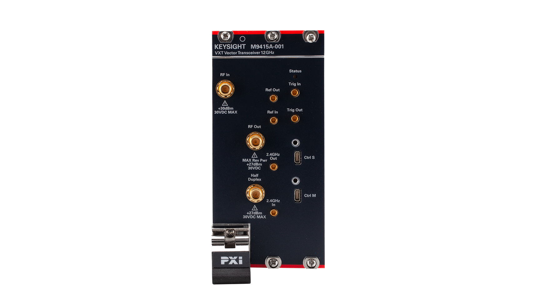
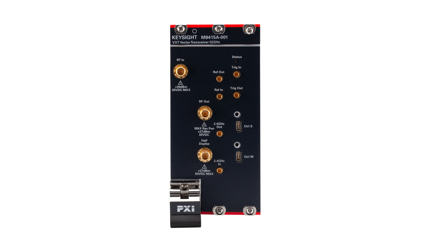
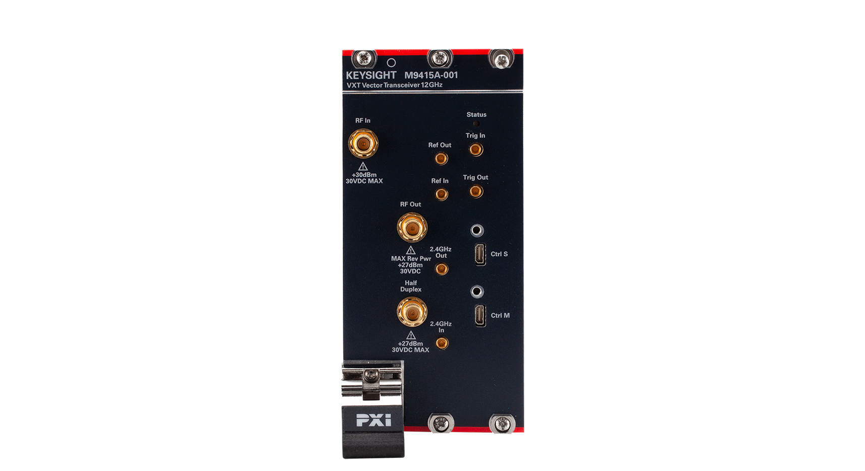
VXT系列M9416A 6GHz至12.3GHz 收发信机 -120dBmto+20dBm 详细指标
Modular PXI RF Vector Transceivers
条件:document are specifications under the following conditions unless otherwise noted.
module, and 20 to 35 °C for environment temperature unless otherwise noted
Specifications describe the warranted performance of calibrated instruments. Data represented in this
• Specifications are valid from 45 to 75 °C for individual module temperature, as reported by the
• Calibrated instrument has been stored for a minimum of 2 hours within the allowed operating range
• If instrument has previously been stored at a temperature range inside the allowed storage range, but
outside the allowed operating range, instrument must have been stored for a minimum of 2 hours
within the allowed operating range before turn-on
• 45-minute warm-up time with the Modular TRX application running
条件:Typical describes additional product performance information that is not covered by the product warranty.
(approximately 25 °C) after alignment within the stated alignment time and temperature limits.
Nominal values indicate expected performance or describe product performance that is useful in the
application of the product but are not covered by the product warranty.
• When used with Keysight M9300A frequency reference and Keysight interconnect cables
• An “All Alignment” has been run within the previous
7 days
• A “Fast Alignment” has been run: o Within the previous 8 hours o If the environmental temperature has changed more than
5°C from the previous Fast Alignment
It is performance beyond specifications that 95 percent of the units exhibit with a
95 percent confidence
level. This data does not include measurement uncertainty and is valid only at room temperature
Recommended best practices in use
• Use slot blockers and EMC filler panels in empty module slots to ensure proper operating
temperatures. Keysight chassis and slot blockers optimize module temperature performance and
• Set chassis fan to high at environmental temperatures above
35 °C.
Standard (Option M02)
256 MSa of IQ data
Option M05
512 MSa of IQ data
Option F06
380 MHz to 6 GHz
Option F08
380 MHz to 8 GHz
Option F12
380 MHz to 12.3 GHz
二、精度, 老化率, 稳定度参见 M9300A 规格
CW ± (marker frequency x frequency reference accuracy + 0.10% x span + 5% x RBW + 2 Hz +
0.5 x
Demodulation ± (center frequency × frequency reference accuracy +
1 Hz)
Standard (Option B4X)
550 MHz to 1.31 GHz
200 MHz
Option B8X
550 MHz to 1.31 GHz
200 MHz
550 MHz to 1.31 GHz
200 MHz
IQ analyzer Free run, External 1, External
2, RF burst, Video, Periodic, PXI, Internal
Trigger delay range
–150 to 500 ms
Option HDX, Half duplex port
+27 dBm
Option HDX, Half duplex port
30 Vdc
Absolute Amplitude Accuracy (CW mode)
1
Frequency Range –70 dBm ≤ Input level < +10 dBm +10 dBm ≤ Input level ≤ +20 dBm +20 dBm < Input level ≤
+27 dBm
380 MHz to 1.31 GHz <
± 0.50 dB
1.31 to 4.3 GHz <
± 0.60 dB
4.3 to 8.4 GHz <
± 0.55 dB
8.4 to 11.4 GHz <
± 0.60 dB
11.4 to 12.3 GHz <
± 0.70 dB
Frequency Range –70 dBm ≤ Input level < +10 dBm +10 dBm ≤ Input level ≤ +20 dBm +20 dBm < Input level ≤
+27 dBm
380 MHz to 1.31 GHz <
± 0.50 dB
1.31 to 4.3 GHz <
± 0.60 dB
4.3 to 8.4 GHz <
± 0.70 dB
8.4 to 11.4 GHz <
± 0.75 dB
11.4 to 12.3 GHz <
± 0.80 dB
Input Voltage Standing Wave Ratio (VSWR)
条件:1. Signal is measured at 1.1 MHz offset from the center frequency, Otherwise, an IF flatness error must be added.
2. Input terminated, LNA on, log power average, and normalized to 1 Hz bandwidth.
RF input port Half Duplex Port (configured to input mode) 380 MHz to 4.3 GHz < 1.55:1, < 1.4:1 typical < 1.55:1, < 1.4:1 typical 4.3 to 5.8 GHz < 1.4:1, < 1.3:1 typical < 1.55:1, < 1.4:1 typical 5.8 to 7.2 GHz < 1.8:1, < 1.6:1 typical < 1.9:1, <
1.7:1 typical
7.2 to 10.2 GHz < 1.6:1, < 1.4:1 typical < 1.6:1, <
1.4:1 typical
10.2 to 12.3 GHz < 2.0:1, < 1.9:1 typical < 2.0:1, <
1.9:1 typical
Displayed Average Noise Floor (DANL)
2
RF input port, with analyzer ranged to –70 dBm Half duplex port (option HDX) with analyzer ranged
to –70 dBm
380 MHz to 4.3 GHz –165 dBm, –167 dBm typical –160 dBm
–162 dBm typical
4.3 to 10.2 GHz –165 dBm, –167 dBm typical –158 dBm
–161 dBm typical
10.2 to 12.3 GHz –162 dBm, –165 dBm typical –155 dBm
–157 dBm typical
Third-order Intermodulation Distortion (TOI, with analyzer ranged to +10 dBm)
380 MHz to 4.3 GHz +30 dBm
+32 dBm typical
4.3 to 6 GHz +28 dBm
+30 dBm typical
6 to 12.3 GHz +27 dBm
+29 dBm typical
Phase Noise Sidebands (CF =
1 GHz)
1 kHz offset –114 dBc/Hz
–116 dBc/Hz typical
10 kHz offset –128 dBc/Hz
–130 dBc/Hz typical
100 kHz offset –132 dBc/Hz
–134 dBc/Hz typical
1 MHz offset –135 dBc/Hz
–137 dBc/Hz typical
10 MHz offset –139 dBc/Hz
–141 dBc/Hz typical
Figure
1. Phase noise from 1 kHz to 10 MHz offset at 1 GHz
RF input port; Option HDX, half duplex port; with analyzer ranged to +10 dBm; offset from 10 MHz to 1/2 × analysis bandwidth
380 MHz to 9 GHz < –79 dBm, <
–82 dBm typical
9 to 9.6 GHz < –76 dBm, <
–80 dBm typical
9.6 to 12.3 GHz < –81 dBm, <
–83 dBm typical
条件:Sideband spurs, nominal 1 kHz to 10 MHz offset –85 dBc
Center frequency 100 MHz BW 200 MHz BW 400 MHz BW 600 MHz BW 800 MHz BW
1.2 GHz BW
380 to 550 MHz
–63 dBc N/A N/A N/A N/A N/A
550 MHz to 1.31 GHz –62 dBc
–60 dBc N/A N/A N/A N/A
s1.31 to 2 GHz –62 dBc –60 dBc –60 dBc
–60 dBc N/A N/A
2 to 4.3 GHz –62 dBc –60 dBc –60 dBc –60 dBc –58 dBc
–56 dBc
4.3 to 4.6 GHz –63 dBc –63 dBc –60 dBc –60 dBc –58 dBc
–56 dBc
4.6 to 12.3 GHz –63 dBc –63 dBc –60 dBc –60 dBc –59 dBc
–58 dBc
RF input port, with analyzer ranged from –30 to +27 dBm
Option HDX, half duplex port, with analyzer ranged from –25 to +27 dBm 380 MHz to 12.3 GHz –52 dBr, –62 dBr typical –52 dBr
–62 dBr typical
条件:1. dBr is LO feedthrough power relative to the range level of the receiver.
RF input port, –25 dBm ≤ Input level ≤
+10 dBm, typical indicated by italics
Center frequency 100 MHz BW 200 MHz BW 400 MHz BW 600 MHz BW 800 MHz BW
1.2 GHz BW
± 0.50 dB N/A N/A N/A N/A N/A
550 MHz to 1.31 GHz
± 0.70 dB
± 0.35 dB
± 0.70 dB,
± 0.40 dB N/A N/A N/A N/A
1.31 to 1.62 GHz
± 0.70 dB
± 0.35 dB
± 0.70 dB,
± 0.40 dB
± 1.20 dB,
± 0.70 dB
± 1.50 dB,
± 0.95 dB N/A N/A
± 0.35 dB
± 0.70 dB,
± 0.40 dB
± 0.65 dB,
± 0.30 dB
± 0.65 dB,
± 0.30 dB N/A N/A
± 0.15 dB
± 0.55 dB,
± 0.25 dB
± 0.65 dB,
± 0.30 dB
± 0.65 dB,
± 0.30 dB
± 0.60 dB,
± 0.25 dB
± 0.75 dB,
± 0.35 dB
± 0.20 dB
± 0.55 dB,
± 0.25 dB
± 0.80 dB,
± 0.40 dB
± 0.80 dB,
± 0.40 dB
± 0.80 dB,
± 0.40 dB
± 0.85 dB,
± 0.45 dB
± 0.50 dB
± 1.00 dB,
± 0.50 dB
± 1.10 dB,
± 0.65 dB
± 1.15 dB,
± 0.70 dB
± 1.15 dB,
± 0.70 dB
± 1.25 dB,
± 0.80 dB
Half duplex port, Option HDX, –25 dBm ≤ Input level ≤
+10 dBm, typical indicated by italics
Center frequency 100 MHz BW 200 MHz BW 400 MHz BW 600 MHz BW 800 MHz BW
1.2 GHz BW
± 0.55 dB N/A N/A N/A N/A N/A
550 MHz to 1.31 GHz
± 0.70 dB
± 0.35 dB
± 0.80 dB,
± 0.40 dB N/A N/A N/A N/A
1.31 to 1.62 GHz
± 0.70 dB
± 0.35 dB
± 0.80 dB,
± 0.40 dB
± 1.15 dB,
± 0.70 dB
± 1.55 dB,
± 0.95 dB N/A N/A
± 0.35 dB
± 0.80 dB,
± 0.40 dB
± 0.60 dB,
± 0.30 dB
± 0.60 dB,
± 0.30 dB N/A N/A
± 0.15 dB
± 0.55 dB,
± 0.25 dB
± 0.60 dB,
± 0.25 dB
± 0.60 dB,
± 0.25 dB
± 0.65 dB,
± 0.30 dB
± 0.70 dB,
± 0.35 dB
± 0.20 dB
± 0.60 dB,
± 0.20 dB
± 0.75 dB,
± 0.40 dB
± 0.75 dB,
± 0.40 dB
± 1.00 dB,
± 0.55 dB
± 1.35 dB,
± 0.80 dB
± 0.40 dB
± 1.00 dB,
± 0.50 dB
± 1.10 dB,
± 0.60 dB
± 1.25 dB,
± 0.70 dB
± 1.30 dB,
± 0.75 dB
± 1.35 dB,
± 0.80 dB
任意波形 sample 存储 (存储 capacity)
Standard (Option M02)
256 MSa of IQ data
Option M05
512 MSa of IQ data
任意波形 sample 存储 (存储 capacity)
Option F06
380 MHz to 6 GHz
Option F08
380 MHz to 8 GHz
Option F12
380 MHz to 12.3 GHz
三、精度, 老化率, 稳定度参见 M9300A 规格
± (output frequency × frequency reference accuracy +
0.001 Hz)
Frequency switching speed
1
Standard (Option B4X)
550 MHz to 1.31 GHz
200 MHz
Option B8X
550 MHz to 1.31 GHz
200 MHz
550 MHz to 1.31 GHz
200 MHz
RF output port 380 MHz to 12.3 GHz
–120 to +5 dBm
Option HDX, half duplex port (configured to output mode) 380 MHz to 12.3 GHz
–120 to +5 dBm
RF output port, Option
1EA
380 MHz to 12.3 GHz –120 to +20 dBm
+25 dBm settable
Option HDX, half duplex port (configured to output mode), Option
1EA
380 MHz to 12.3 GHz
–120 to +10 dBm
条件:1. Switching speed depends highly upon the hardware and controller that is used. Measurements were made with the M9416A in an
M9018B chassis with the M9037A embedded controller, Windows 10 Operating System.
Average power input
+27 dBm
Amplitude switching speed
1
Figure
2. Measured relative level accuracy at 1 GHz
RF 输出端口, 典型值 indicated by italics
550 MHz
550 MHz to
4.3 GHz 4.3 to 6 GHz 6 to 7.8 GHz
7.8 to
10.2 GHz
10.2 to
12.3 GHz
+10 dBm
≤ +20 dBm
0 dBm
≤ +10 dBm
–60 dBm
≤ 0 dBm
–90 dBm
< –60 dBm
–100 dBm
< –90 dBm
–110 dBm
< –100 dBm
Option HDX, half duplex port, typical indicated by italics
Frequency range 380 to 550 MHz 550 MHz to4.3 GHz 4.3 to 6 GHz 6 to 7.8 GHz 7.8 to 10.2 GHz
10.2 to 12.3 GHz
0 dBm
≤ +10 dBm
–60 dBm
≤ 0 dBm
–90 dBm
< –60 dBm
–100 dBm
< –90 dBm
–110 dBm
< –100 dBm
条件:Delta from initial value < ± 0.10 dB nominal
RF output port, 0 dBm output power, 1 GHz
25 °C
Setting resolution
0.01 dB
Output Voltage Standing Wave Ratio (VSWR)
RF output port 380 MHz to 1.31 GHz < 1.90:1, < 1.70:1 typical 1.31 to 7.8 GHz < 1.75:1, < 1.65:1 typical 7.8 to 10.2 GHz < 1.75:1, <
1.60:1 typical
10.2 to 12.3 GHz < 2.00:1, <
1.70:1 typical
Option HDX, half duplex port (configured to output mode) 380 MHz to 1.31 GHz < 1.90:1, < 1.75:1 typical 1.31 to 6 GHz < 1.75:1, < 1.40:1 typical 6 to 10.2 GHz < 1.65:1, <
1.50:1 typical
10.2 to 12.3 GHz < 1.90:1, <
1.55:1 typical
条件:+10 dBm output power, with Option 1EA
RF output port 0 dBm output power 380 MHz to 4.3 GHz < –41 dBc, < –45 dBc typical 4.3 to 5.8 GHz < –36 dBc, <
–42 dBc typical
5.8 to 10.2 GHz < –34 dBc, <
–39 dBc typical
10.2 to 12.3 GHz < –41 dBc, <
–46 dBc typical
380 MHz to 4.3 GHz < –31 dBc, <
–35 dBc typical
4.3 to 5.8 GHz < –27 dBc, <
–33 dBc typical
5.8 to 9 GHz < –26 dBc, <
–31 dBc typical
9 to 10.2 GHz < –24 dBc, <
–29 dBc typical
10.2 to 12.3 GHz < –29.5 dBc, <
–35 dBc typical
Option HDX, half duplex port
–5 dBm output power
380 MHz to 4.3 GHz < –36 dBc, <
–40 dBc typical
4.3 to 5.8 GHz < –33 dBc, <
–38 dBc typical
5.8 to 10.2 GHz < –32 dBc, <
–37 dBc typical
10.2 to 12.3 GHz < –36 dBc, <
–42 dBc typical
RF output port, Option HDX, half duplex port
0 dBm output power
380 MHz to 4.3 GHz < –65 dBc, <
–70 dBc typical
4.3 to 6.5 GHz < –47 dBc, <
–52 dBc typical
6.5 to 9.6 GHz < –57 dBc, <
–62 dBc typical
9.6 to 11.4 GHz < –50 dBc, <
–56 dBc typical
11.4 to 12.3 GHz < –51 dBc, <
–60 dBc typical
RF output port, Option HDX, half duplex port
0 dBm output power
380 MHz to 1.31 GHz –51 dBc
–65 dBc typical
1.31 to 1.62 GHz –46 dBc
–59 dBc typical
1.62 to 2 GHz –44 dBc
–58 dBc typical
2 to 4.3 GHz –42 dBc
–54 dBc typical
4.3 to 12.3 GHz –46 dBc
–52 dBc typical
RF output port
0 dBm output power, typical indicated by italics
Center frequency 100 MHz BW 200 MHz BW 400 MHz BW 600 MHz BW 800 MHz BW
1.2 GHz BW
–61 dBc N/A N/A N/A N/A N/A
550 MHz to 1.31 GHz
–54 dBc
–60 dBc
–54 dBc,
–59 dBc N/A N/A N/A N/A
–59 dBc
–52 dBc,
–58 dBc
–51 dBc,
–57 dBc
–49 dBc,
–54 dBc N/A N/A
–58 dBc
–51 dBc,
–57 dBc
–51 dBc,
–54 dBc
–50 dBc,
–54 dBc
–49 dBc,
–53 dBc
–46 dBc,
–50 dBc
Option HDX, half duplex port
0 dBm output power, typical indicated by italics
Center frequency 100 MHz BW 200 MHz BW 400 MHz BW 600 MHz BW 800 MHz BW
1.2 GHz BW
–61 dBc N/A N/A N/A N/A N/A
550 MHz to 1.31 Hz
–54 dBc
–60 dBc
–53 dBc,
–57 dBc N/A N/A N/A N/A
–58 dBc
–50 dBc,
–57 dBc
–50 dBc,
–56 dBc
–49 dBc,
–55 dBc N/A N/A
–57 dBc
–49 dBc,
–58 dBc
–48 dBc,
–54 dBc
–48 dBc,
–53 dBc
–47 dBc,
–51 dBc
–45 dBc,
–48 dBc
RF output port, Option HDX, half duplex port
0 dBm output power
Offset 380 MHz to 4.3 GHz 4.3 to 6 GHz 6 to 10.2 GHz
10.2 to 12.3 GHz
–76 dBc typical
–66 dBc,
–72 dBc typical
–62 dBc,
–69 dBc typical
–60 dBc,
–65 dBc typical
–95 dBc typical
–86 dBc,
–92 dBc typical
–84 dBc,
–89 dBc typical
–70 dBc,
–75 dBc typical
–96 dBc typical
–88 dBc,
–94 dBc typical
–87 dBc,
–93 dBc typical
–81 dBc,
–86 dBc typical
条件:1. Measured at 10.1 MHz offset from the center frequency.
RF output port, 0 dBm; Option HDX, half duplex port, 0 dBm; Option 1EA, +10 dBm; Center frequency =
1 GHz
1 kHz offset –105 dBc/Hz
–115 dBc/Hz typical
10 kHz offset –126 dBc/Hz
–133 dBc/Hz typical
100 kHz offset –134 dBc/Hz
–139 dBc/Hz typical
1 MHz offset –141 dBc/Hz
–145 dBc/Hz typical
10 MHz offset –142 dBc/Hz
–145 dBc/Hz typical
Figure 3. Measured phase noise from 1 kHz to 10 MHz offset at 1, 3, 5
7.2 and 12 GHz
RF output port, output level =
0 dBm
380 to 550 MHz –131 dBm/Hz
–135 dBm/Hz typical
550 MHz to 4.3 GHz –133 dBm/Hz
–137 dBm/Hz typical
4.3 to 10.2 GHz –131 dBm/Hz
–135 dBm/Hz typical
10.2 to 12.3 GHz –133 dBm/Hz
–136 dBm/Hz typical
Option HDX, half duplex port, output level =
–10 dBm
380 to 550 MHz –142 dBm/Hz
–147 dBm/Hz typical
550 MHz to 4.3 GHz –143 dBm/Hz
–147 dBm/Hz typical
4.3 to 10.2 GHz –139 dBm/Hz
–144 dBm/Hz typical
10.2 to 12.3 GHz –141 dBm/Hz
–145 dBm/Hz typical
RF output port, output level =
0 dBm
380 MHz to 7.8 GHz +24 dBm
+27 dBm typical
7.8 to 10.2 GHz +23 dBm
+25 dBm typical
10.2 to 12.3 GHz +21 dBm
+24 dBm typical
Option HDX, half duplex port, output level =
0 dBm
380 to 550 MHz +25 dBm
+28 dBm typical
550 MHz to 4.3 GHz +23 dBm
+26 dBm typical
4.3 to 7.8 GHz +20 dBm
+24 dBm typical
7.8 to 10.2 GHz +18 dBm
+22 dBm typical
10.2 to 12.3 GHz +17 dBm
+20 dBm typical
RF output port, –30 dBm ≤ Level ≤ +10 dBm, sample rate =
1.25 x bandwidth, typical indicated by italics
Center frequency 100 MHz BW 200 MHz BW 400 MHz BW 600 MHz BW 800 MHz BW
1.2 GHz BW
± 0.35 dB N/A N/A N/A N/A N/A
± 0.25 dB
± 0.80 dB,
± 0.40 dB N/A N/A N/A N/A
± 0.25 dB
± 0.80 dB,
± 0.45 dB N/A N/A N/A N/A
730 MHz to 1.31 GHz
± 0.65 dB
± 0.40 dB
± 0.75 dB,
± 0.45 dB N/A N/A N/A N/A
1.31 to 1.62 GHz
± 0.75 dB
± 0.40 dB
± 0.80 dB,
± 0.40 dB
± 1.10 dB,
± 0.75 dB
± 1.25 dB,
± 0.90 dB N/A N/A
± 0.20 dB
± 0.65 dB,
± 0.30 dB
± 0.65 dB,
± 0.25 dB
± 0.80 dB,
± 0.45 dB N/A N/A
± 0.30 dB
± 0.75 dB,
± 0.45 dB
± 0.75 dB,
± 0.45 dB
± 0.75 dB,
± 0.45 dB
± 0.75 dB,
± 0.45 dB
± 0.85 dB,
± 0.55 dB
± 0.25 dB
± 0.65 dB,
± 0.25 dB
± 0.90 dB,
± 0.60 dB
± 1.25 dB,
± 0.85 dB
± 1.25 dB,
± 0.85 dB
± 1.30 dB,
± 0.90 dB
± 0.40 dB
± 0.80 dB,
± 0.45 dB
± 0.85 dB,
± 0.50 dB
± 0.80 dB,
± 0.55 dB
± 0.80 dB,
± 0.55 dB
± 1.20 dB,
± 0.85 dB
± 0.30 dB
± 0.75 dB,
± 0.30 dB
± 0.75 dB,
± 0.30 dB
± 0.70 dB,
± 0.40 dB
± 0.75 dB,
± 0.40 dB
± 0.80 dB,
± 0.50 dB
± 0.20 dB
± 0.70 dB,
± 0.25 dB
± 0.70 dB,
± 0.35 dB
± 0.80 dB,
± 0.40 dB
± 0.85 dB,
± 0.45 dB
± 1.30 dB,
± 0.75 dB
10.2 to 12.3 GHz
± 0.80 dB
± 0.40 dB
± 0.80 dB,
± 0.45 dB
± 0.85 dB,
± 0.50 dB
± 0.90 dB,
± 0.60 dB
± 0.90 dB,
± 0.60 dB
± 0.90 dB,
± 0.60 dB
Half duplex port, Option HDX, –20 dBm ≤ Level ≤ +5 dBm, sample rate =
1.25 x bandwidth, typical indicated by italics
Center frequency 100 MHz BW 200 MHz BW 400 MHz BW 600 MHz BW 800 MHz BW
1.2 GHz BW
± 0.35 dB N/A N/A N/A N/A N/A
± 0.25 dB
± 0.70 dB,
± 0.40 dB N/A N/A N/A N/A
± 0.25 dB
± 0.70 dB,
± 0.40 dB N/A N/A N/A N/A
730 MHz to 1.31 GHz
± 0.65 dB
± 0.45 dB
± 0.75 dB,
± 0.50 dB N/A N/A N/A N/A
1.31 to 1.62 GHz
± 0.70 dB
± 0.35 dB
± 0.75 dB,
± 0.40 dB
± 1.00 dB,
± 0.70 dB
± 1.15 dB,
± 0.85 dB N/A N/A
± 0.25 dB
± 0.65 dB,
± 0.25 dB
± 0.60 dB,
± 0.20 dB
± 0.50 dB,
± 0.35 dB N/A N/A
± 0.30 dB
± 0.65 dB,
± 0.40 dB
± 0.65 dB,
± 0.40 dB
± 0.65 dB,
± 0.45 dB
± 0.65 dB,
± 0.45 dB
± 0.65 dB,
± 0.45 dB
± 0.35 dB
± 0.65 dB,
± 0.35 dB
± 0.70 dB,
± 0.45 dB
± 0.75 dB,
± 0.50 dB
± 0.80 dB,
± 0.55 dB
± 0.80 dB,
± 0.55 dB
± 0.30 dB
± 0.70 dB,
± 0.45 dB
± 0.85 dB,
± 0.50 dB
± 0.75 dB,
± 0.55 dB
± 0.75 dB,
± 0.55 dB
± 1.10 dB,
± 0.85 dB
± 0.35 dB
± 0.65 dB,
± 0.35 dB
± 0.70 dB,
± 0.40 dB
± 0.70 dB,
± 0.40 dB
± 0.70 dB,
± 0.45 dB
± 0.75 dB,
± 0.50 dB
± 0.20 dB
± 0.65 dB,
± 0.30 dB
± 0.80 dB,
± 0.55 dB
± 0.80 dB,
± 0.65 dB
± 1.00 dB,
± 0.75 dB
± 1.15 dB,
± 0.75 dB
10.2 to 12.3 GHz
± 0.55 dB
± 0.20 dB
± 0.65 dB,
± 0.30 dB
± 0.80 dB,
± 0.45 dB
± 0.75 dB,
± 0.50 dB
± 0.80 dB,
± 0.55 dB
± 0.80 dB,
± 0.50 dB
条件:Connector: MMPX female, 50 Ω nominal
Input amplitude: >+10 dBm, nominal
Output amplitude: >+10 dBm, nominal
Connector: MMPX female, 50 Ω nominal
Input amplitude: >+10 dBm, nominal
Output amplitude: >+12 dBm, nominal
Lock range
± 1 ppm, nominal
LO reference 2.4 GHz In
2.4 GHz Out
条件:Input impedance: 1 kΩ or 50 Ω nominal
Input level range
0 to +3.3 V
Output impedance
50 Ω nominal
Output level range
3.3 V LVTTL
Ctrl M, Ctrl S Connector: Micro-HDMI female
Level range
3.3 V LVTTL, LVDS
Operating temperature
0 to +45 °C
Storage temperature
–40 to +65 °C
Complies with European EMC Directive
2014/30/EU
• CISPR 11, Group
1, Class A
• ICES/NMB-001
This ISM device complies with Canadian ICES-001
Cet appareil ISM est conforme a la norme NMB-001 du Canada
条件:conditions; test methods are aligned with IEC 60068-2 and levels are similar to MILPRF-28800F Class 3.
Samples of this product have been type tested in accordance with the Keysight Environmental Test Manual
and verified to be robust against the environmental stresses of storage, transportation, and end-use; those
stresses include, but are not limited to, temperature, humidity, shock, vibration, altitude, and power line
H x W x D 130.2 mm x 80.8 mm x
209.6 mm
The VXT PXIe vector transceiver is supplied with a
1-year warranty
The recommended calibration cycle is one year; calibration services are available through Keysight service centers
五、WLAN 测量 Application 主要指标
条件:EVM floor conditions Phase Tracking on, Eq Smoothing on, Eq Training Seq only, RF output loopback to RF input, at –20 dBm
input power, optimized range, nominal 802.11ac 5.8 GHz 80 MHz < –51 dB 802.11ac 5.8 GHz 160 MHz < –50 dB 802.11ax 5.8 GHz 80 MHz < –52 dB
EVM floor conditions Phase Tracking on, Eq Smoothing on, Eq Training Seq only, RF output loopback to RF input, at –15 dBm
input power, optimized range, nominal rms-EVM nc-EVM 1 802.11be, 5 GHz, 160 MHz, 1024 QAM < –50 dB 802.11be, 5.8 GHz, 160 MHz, 1024 QAM < –51 dB
802.11ax 5.8 GHz 160 MHz <
–50 dB
802.11ax 7 GHz 80 MHz <
–51 dB
802.11ax 7 GHz 160 MHz <
–50 dB
802.11be, 7 GHz, 160 MHz, 1024 QAM <
–50 dB
802.11be, 5 GHz, 320 MHz, 4096 QAM < –46 dB <
–51.9 dB
802.11be, 5.8 GHz, 320 MHz, 4096 QAM < –47 dB <
–52.0 dB
802.11be, 7 GHz, 320 MHz, 4096 QAM < –47 dB <
–51.9 dB
条件:RF output port, at –5 dBm to –15 dBm output power, nominal
EVM floor conditions Phase Tracking on, Eq Smoothing on, Eq Training Seq only, RF output loopback to RF input, at –15 dBm
input power, optimized range, nominal rms-EVM nc-EVM 802.11be, 5 GHz, 160 MHz, 1024 QAM < –50 dB 802.11be, 5.8 GHz, 160 MHz, 1024 QAM < –51 dB
1. nc-EVM: noise corrected EVM, is a technique to improve EVM by compensating analyzer’s noise in EVM domain.
802.11ac 5.8 GHz 80 MHz <
–51 dB
802.11ac 5.8 GHz 160 MHz <
–50 dB
802.11ax 5.8 GHz 80 MHz <
–52 dB
802.11ax 5.8 GHz 160 MHz <
–50 dB
802.11ax 7 GHz 80 MHz <
–51 dB
802.11ax 7 GHz 160 MHz <
–49 dB
802.11be, 7 GHz, 160 MHz, 1024 QAM <
–50 dB
802.11be, 5 GHz, 320 MHz, 4096 QAM < –46 dB <
–51.9 dB
802.11be, 5.8 GHz, 320 MHz, 4096 QAM < –47 dB <
–52.0 dB
802.11be, 7 GHz, 320 MHz, 4096 QAM < –47 dB <
–51.9 dB
Figure 4. WLAN
802.11ax EVM vs. output power level at 5.8 GHz, loopback
Figure 5. WLAN
802.11be EVM vs. output power level at 7 GHz, loopback
5G NR Measurement Application Key Specifications
条件:120 kHz SCS, 4 GHz, 200 MHz (256QAM) 0.28% nominal
120 kHz SCS, 5 GHz, 200 MHz (256QAM) 0.36% nominal
120 kHz SCS, 7 GHz, 200 MHz (256QAM) 0.35% nominal
120 kHz SCS, 12.3 GHz, 200 MHz (256QAM) 0.41% nominal
120 kHz SCS, 4 GHz, 400 MHz (256QAM) 0.42% nominal
120 kHz SCS, 5 GHz, 400 MHz (256QAM) 0.50% nominal
120 kHz SCS, 7 GHz, 400 MHz (256QAM) 0.43% nominal
120 kHz SCS, 11 GHz, 400 MHz (256QAM) 0.50% nominal
120 kHz SCS, 7 GHz, 100 MHz 8CC (256QAM) 0.65% nominal
120 kHz SCS, 12.3 GHz, 100 MHz 8CC (256QAM) 0.74% nominal
Residual EVM, at -10 dBm or 0 dBm input power
30 kHz SCS, 4 GHz, 100 MHz (256QAM)
0.33%
30 kHz SCS, 5 GHz, 100 MHz (256QAM)
0.38%
30 kHz SCS, 7 GHz, 100 MHz (256QAM)
0.46%
30 kHz SCS, 12 GHz, 100 MHz (256QAM)
0.42%
Residual EVM, RF output loopback to RF input, at -5 dBm input power
Residual EVM, RF output loopback to RF input, at -5 dBm input power
RF input port, at -10 dBm or 0 dBm input power, LNA off, noise correction on
30 kHz SCS, 4 GHz, 100 MHz (256QAM)
–66 dBc typical
30 kHz SCS, 5 GHz, 100 MHz (256QAM)
–66 dBc typical
Figure 6.
5G NR downlink ACP vs. input power level at RF input port, LNA off
5G NR Source Key Specifications
Modulation signal level accuracy 600 MHz to 12.3 GHz
± 0.45 dB
条件:120 kHz SCS, 4 GHz, 200 MHz (256QAM) 0.28% nominal
120 kHz SCS, 5 GHz, 200 MHz (256QAM) 0.36% nominal
120 kHz SCS, 7 GHz, 200 MHz (256QAM) 0.35% nominal
120 kHz SCS, 12.3 GHz, 200 MHz (256QAM) 0.41% nominal
120 kHz SCS, 4 GHz, 400 MHz (256QAM) 0.42% nominal
120 kHz SCS, 5 GHz, 400 MHz (256QAM) 0.50% nominal
120 kHz SCS, 7 GHz, 400 MHz (256QAM) 0.43% nominal
120 kHz SCS, 11 GHz, 400 MHz (256QAM) 0.50% nominal
120 kHz SCS, 7 GHz, 100 MHz 8CC (256QAM) 0.65% nominal
120 kHz SCS, 12.3 GHz, 100 MHz 8CC (256QAM) 0.74% nominal
Composite EVM, RF output port, half duplex port, at –10 dBm output power
30 kHz SCS, 4 GHz, 100 MHz (256QAM) 0.28%
0.24% typical
30 kHz SCS, 5 GHz, 100 MHz (256QAM) 0.28%
0.26% typical
30 kHz SCS, 7 GHz, 100 MHz (256QAM) 0.30%
0.27% typical
30 kHz SCS, 12 GHz, 100 MHz (256QAM) 0.40%
0.35% typical
Composite EVM, RF output port, at 0 dBm output power
30 kHz SCS, 4 GHz, 100 MHz (256QAM) 0.33%
0.28% typical
30 kHz SCS, 5 GHz, 100 MHz (256QAM) 0.33%
0.29% typical
30 kHz SCS, 7 GHz, 100 MHz (256QAM) 0.33%
0.29% typical
30 kHz SCS, 12 GHz, 100 MHz (256QAM) 0.67%
0.56% typical
Composite EVM, RF output port loopback to RF input, at –5 dBm output power
Composite EVM, RF output port loopback to RF input, at –10 dBm output power
Figure 7.
5G NR downlink ACP vs. input power level at RF input port, LNA on
条件:120 kHz SCS, 4 GHz, 200 MHz (256QAM) –58.0 dBc nominal
120 kHz SCS, 5 GHz, 200 MHz (256QAM) –54.0 dBc nominal
120 kHz SCS, 7 GHz, 200 MHz (256QAM) –56.5 dBc nominal
120 kHz SCS, 11 GHz, 200 MHz (256QAM) –54.5 dBc nominal
120 kHz SCS, 4 GHz, 400 MHz (256QAM) –54.0 dBc nominal
120 kHz SCS, 5 GHz, 400 MHz (256QAM) –51.0 dBc nominal
120 kHz SCS, 7 GHz, 400 MHz (256QAM) –52.0 dBc nominal
120 kHz SCS, 11 GHz, 400 MHz (256QAM) –52.0 dBc nominal
120 kHz SCS, 7 GHz, 100 MHz 8CC (256QAM) –50.5 dBc nominal
120 kHz SCS, 11 GHz, 100 MHz 8CC (256QAM) –49.0 dBc nominal
RF output port, at –10 dBm output power
30 kHz SCS, 4 GHz, 100 MHz (256QAM) –59.5 dBc
–60.5 dBc typical
30 kHz SCS, 5 GHz, 100 MHz (256QAM) –55.0 dBc
–56.0 dBc typical
30 kHz SCS, 7 GHz, 100 MHz (256QAM) –57.0 dBc
–58.0 dBc typical
30 kHz SCS, 12 GHz, 100 MHz (256QAM) –53.0 dBc
–55.5 dBc typical
RF output port, at 0 dBm output power
30 kHz SCS, 4 GHz, 100 MHz (256QAM) 0.33%
0.28% typical
30 kHz SCS, 5 GHz, 100 MHz (256QAM) 0.33%
0.29% typical
30 kHz SCS, 7 GHz, 100 MHz (256QAM) 0.33%
0.29% typical
30 kHz SCS, 12 GHz, 100 MHz (256QAM) 0.67%
0.56% typical
RF output port, at –10 dBm output power
Figure 8. 5G NR downlink ACP vs. output power level, 100 MHz bandwidth, 30 kHz SCS
256 QAM
Figure 9. 5G NR downlink EVM vs. output power level, LNA off, loopback, with 100 MHz bandwidth, 30 kHz SCS
256 QAM
Figure 10. 5G NR downlink EVM vs. output power level, LNA on, loopback, with 100 MHz bandwidth, 30 kHz SCS
256 QAM
LTE/LTE-Advanced FDD & LTE/LTE-Advanced TDD
Measurement Application Key Specifications
1
条件:1. For frequencies from 695 to 3800 MHz
Residual EVM, at –10 dBm or 0 dBm input power
900 MHz 5 MHz bandwidth 0.21% downlink
0.19% uplink
20 MHz bandwidth 0.24% downlink
0.26% uplink
2000 MHz 5 MHz bandwidth 0.21% downlink
0.22% uplink
20 MHz bandwidth 0.29% downlink
0.26% uplink
RF input port; Half duplex port (option HDX); at –10 dBm or 0 dBm input power
FDD E-UTRA (Uplink and Downlink) 900 MHz 5 MHz bandwidth –63 dBc typical 2000 MHz
20 MHz bandwidth
FDD UTRA (Uplink and Downlink 900 MHz 5 MHz bandwidth –69 dBc typical 2000 MHz
20 MHz bandwidth
TDD E-UTRA (Uplink and Downlink) 900 MHz 5 MHz bandwidth –62 dBc typical 2000 MHz
20 MHz bandwidth
TDD UTRA (Uplink and Downlink 900 MHz 5 MHz bandwidth –68 dBc typical 2000 MHz
20 MHz bandwidth
Modulated signal level accuracy 410 MHz to 3.3 GHz ± 0.51 dB 3.3 to 5.8 GHz
± 0.66 dB
Residual EVM, at –10 dBm or 0 dBm output power
FDD 900 MHz 5 MHz bandwidth < 0.24% 20 MHz bandwidth < 0.35% 2000 MHz 5 MHz bandwidth <
0.28%
20 MHz bandwidth <
0.39%
TDD 900 MHz 5 MHz bandwidth < 0.32% 20 MHz bandwidth < 0.29% 2000 MHz 5 MHz bandwidth <
0.35%
20 MHz bandwidth <
0.34%
RF input port; Half duplex port (option HDX); at –10 dBm output power Adjacent Alternate
FDD 900 MHz 5 MHz bandwidth –67 dBc –69 dBc 20 MHz bandwidth –62 dBc –63 dBc 2000 MHz 900 MHz –66 dBc
–70 dBc
TDD 900 MHz 5 MHz bandwidth –66 dBc –68 dBc 20 MHz bandwidth –62 dBc –63 dBc 2000 MHz 900 MHz –65 dBc
–69 dBc
RF input port; Half duplex port (option HDX); at –0 dBm output power Adjacent Alternate
FDD 900 MHz 5 MHz bandwidth –64 dBc –68 dBc 20 MHz bandwidth –62 dBc –62 dBc 2000 MHz 5 MHz bandwidth –63 dBc
–70 dBc
20 MHz bandwidth –62 dBc
–66 dBc
TDD 900 MHz 5 MHz bandwidth –63 dBc –68 dBc 20 MHz bandwidth –62 dBc –63 dBc 2000 MHz 5 MHz bandwidth –62 dBc
–70 dBc
20 MHz bandwidth –62 dBc
–66 dBc
W-CDMA/HSPA+ Measurement Application Key
Adjacent Channel Power Ratio (ACPR)
条件:5 MHz offset –66 dBc nominal at 0 dBm input power
Residual relative power in 3.84 MHz BW
Spectrum Emission Mask (SEM)
条件:Downlink 2.515 to 2.715 MHz –83 dBc nominal in a 30 kHz BW 2.715 to 3.515 MHz –85 dBc nominal in a 1 MHz BW 3.515 to 4 MHz –85 dBc nominal in a 1 MHz BW
4 to 8 MHz –71 dBc nominal in a 1 MHz BW
8 to 12.5 MHz –72 dBc nominal in a 1 MHz BW
Uplink 2.515 to 3.485 MHz –84 dBc nominal in a 30 kHz BW 4 to 7.5 MHz –72 dBc nominal in a 1 MHz BW 7.5 to 8.5 MHz –73 dBc nominal in a 1 MHz BW
8.5 to 12 MHz –73 dBc nominal in a 1 MHz BW
Residual relative power (offset), at 0 dBm input power
Spectrum Emission Mask (SEM) · W-CDMA/HSPA+ Source Key Specifications
Error Vector Magnitude (EVM)
2
Composite EVM, RF output port, half duplex port, at 0 dBm output power
Adjacent Channel Leakage Ratio (ACLR), RF output port, half duplex port, at 0 dBm output power
Offset Configuration Frequency (MHz) ACLR
条件:Adjacent 5 MHz 1800 to 2000 –65 dB nominal
Adjacent 5 MHz 1800 to 2000 –66 dB nominal
2. For frequencies from 730 to 2650 MHz
Adjacent 10 MHz
–69 dB nominal
Adjacent 10 MHz
–71 dB nominal
Adjacent 10 MHz
–69 dB nominal
Adjacent 10 MHz
–72 dB nominal
Keysight enables innovators to push the boundaries of engineering by quickly solving
design, emulation, and test challenges to create the best product experiences. Start your
This information is subject to change without notice. © Keysight Technologies, 2022 - 202
4
Published in USA, December 10 , 202 4, 3122
-2221 .EN
条件:For more detailed product and specification information refer to the following literature and web pages:
• M9416A VXT PXIe Vector Transceiver Configuration Guide (literature no.
3122-2155.EN)
• M9300A PXIe Frequency Reference Data Sheet (literature no.
5991-0898EN)
• M9018B and M9019A PXIe 18 slot Chassis Data Sheet (literature no.
5992-1481EN)
• M9038A PXIe Embedded Controller Data Sheet (literature no.
3122-1717.EN)
• X-Series Measurement Applications Brochure (literature no.
5989-8019EN)
• Signal Studio Software Brochure (literature no.
5989-6448EN)
以上指标摘自厂家官方数据手册,完整定义、测试条件与保证值口径以手册为准。完整指标、测试条件与定义口径请见产品页「软件和手册 | 白皮书」栏目中的官方数据手册。
是德科技 | KEYSIGHT · onetest 仪器资源库


 客服








 粤公网安备44030902003758