是德科技 | KEYSIGHT
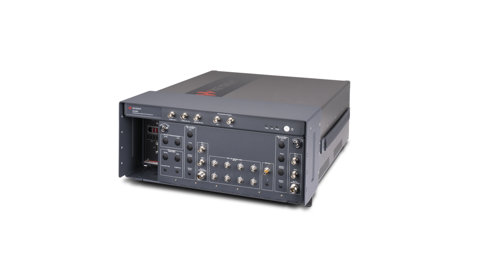
S9108A 6GHz 收发信机 600MHz 详细指标
Wideband RF transceiver testing
条件:The nominal insertion loss of the passive components is as follows:
Based on these insertion losses, the expected source power levels for the blocker system are as follows:
The basic RF performance of the 5G Multi-port FR1 Solution with Blocker is expected to be similar to the
performance of the M9410A/M9411A VXT PXI transceivers, subject to the additional insertion loss of the
passive components (coupler, combiner, switches, attenuators, cables, and connectors/adapters) in the
• Main source output path, from Main M9411A VXT front panel to DUT connector on system
• Blocker source output path, from Blocker M9410A VXT front panel to DUT connector on
• Main VXT Half Duplex path, from Main M9411A VXT front panel to HD port on system front
• Blocker VXT Half Duplex path, from Blocker M9410A VXT front panel to HD port on system
• CW source path, from Aux I/O connector to DUT connector
17.9 dB
• Receiver normal path, from system front panel DUT connector to Main M9411A VXT front
• Receiver low loss path, from system front panel DUT connector to Main M9411A VXT front
• Max Main VXT output power at DUT connector on system front panel
2 dBm
• Max Blocker VXT output power at DUT connector on system front panel
-12 dBm
• Max Main VXT output power at HD port on system front panel
4 dBm
• Max Blocker VXT output power at HD port on system front panel
4 dBm
• CW source output power at DUT connector on system front panel
2.1 dBm
Amplitude correction of these insertion loss have been settled in the S9108A firmware. Users are not
适用型号 S9108A Configurations
This data sheet contains system performance for the S9108A base system that is available in the
following four standard configurations
• S9108A-001
5G FR1 Multi-port Vector Transceiver
• S9108A-002
5G FR1 Multi-port Vector Transceiver with Blocker Solution
• S9108A-003 5G FR1 Multi-port Transceiver Solution with Blocker and HD Port MIMO
• S9108A-006: 5G FR1 Multi-port Transceiver
600 MHz BW with Blocker and HD Port MIMO
Figure 1. Block diagram of S9108A-002, S9108A-003, and S9108A-006
5G multi-port FR1 Solution with
条件:low-loss path is provided to facilitate measurements of Transmit On/Off Power.
An Aux I/O port is shown in the diagram for connecting an additional CW source.
The Aux I/O port can also be used to connect a separate spectrum analyzer.
Figure 1 shows the block diagram of the S9108A-002, S9108A-003, and S9108A-006
5G FR1 multi-port
solution with Blocker. These systems provide a Main VXT for generating the “wanted” signal and a
Blocker VXT for generating the interfering signal for testing the receiver of a base station. Both signals
are combined and available at the system’s test ports. The receiver of the Main VXT, M9411A is used for
all signal analysis measurements. The switching/signal conditioning components shown in the shaded
box provide signal routing and switching to 8 bidirectional RF ports for connection to the base station
under test, with attenuation to protect the VXT modules from the base station’s high transmit power. A
Not Included in S9108A-001
*
*
*
*
Half-Duplex (HD) port connections are provided on the front panel to connect to the HD ports on the Main
and Blocker (M9410A) VXTs. The HD Port 1 for the Main VXT is used for system calibration. Optionally
HD Port 2 can be used in combination with HD Port 1 to make
2x2 MIMO measurements on S9108A-003
and S9108A-006 model configurations, subject to the following:
• Since the ports are half-duplex, they can only be used as either Tx or Rx ports. Simultaneous MIMO
signal generation and analysis are not supported
• MIMO operation requires option MMO, Timing Synchronization for MIMO, to be installed on each
VXT module. This option is not included in the S9108A-002 system.
条件:with 89601200C and 89601BHNC licenses are required for 5G NR MIMO measurements and need to be purchased separately.
The Y9085EM0E 5G NR Waveform and Measurement Application does not support MIMO measurements. The
89600 VSA software
The signal generation and analysis capabilities of the blocker system are based on the hardware
characteristics of the M9410A and M9411A VXT PXIe vector transceivers, in combination with the Signal
Studio and 5G NR measurement software applications. The blocker system is designed to perform most
in-band conducted FR1 transmitter tests for Local Area Base Stations as specified in 3GPP TS
38.141-1
Chapter
6, with the following limitations:
• 6.4 Transmit ON/OFF power: System noise floor is about
-100 dBm/MHz at some frequencies
which may not be adequate to verify the OFF power level in some cases, depending on the base
• 6.6.5 Transmitter spurious emissions: Not supported. Test requires measurement up to 12.75
GHz which is beyond the frequency range of the M9411A, and system dynamic range/spurious
performance may not be adequate for some measurements
• 6.7 Transmitter intermodulation: Not supported. Test requires high power interfering signal and
circulator, 和 out-of-频段杂散测量
条件:Chapter 7, the blocker system can be used for most of the tests, with the following limitations:
AWGN by playing back a waveform file, but it does not support real-time AWGN.
analyzer can be connected to the system using the Aux I/O port to perform this test.
All S9108A models provide single channel measurements only at the 8 RF DUT ports.
For conducted FR1 testing of the receiver for Local Area Base Stations as specified in 3GPP TS
38.141-1
• 7.3 Dynamic Range: This test requires AWGN as the interfering signal. The system can generate
• 7.6 Receiver Spurious Emissions: Not supported. This requires a microwave spectrum analyzer
that can measure beyond the frequency range of the blocker system. A customer-supplied spectrum
The systems cover testing of single carrier signal configurations. Some carrier aggregation configurations
are also covered, but there may be more complex configurations (e.g. non-contiguous carrier
aggregation) that are not supported
The blocker system is NOT intended for testing of Wide Area or Medium Range Base Stations, which
require input/output power levels that may exceed the capabilities of this system and could damage the
条件:components. There is no system-level calibration for the complete solution.
Periodic calibration/recertification of the blocker system consists of calibration of the individual system
All S9108A Standard Configurations RF
Transceiver RF I/O ports and HD Ports
380 to 6000 MHz
适用型号 S9108A-001, S9108A-002, S9108A-003
Configurations 380 to 550 MHz 100 MHz 550 to 1310 MHz 200 MHz 1310 to 6000 MHz
300 MHz
适用型号 S9108A-006 Configuration
All S9108A Standard Configurations RF
Transceiver RF I/O ports
+33 dBm
Half Duplex Connector
+27 dBm
All S9108A Standard Configurations RF
Frequency Range Level Accuracy 380 to 3000 MHz -40 to -10 dBm ≤ ± 0.85 dB, ≤ ± 0.40 dB (typical) 3000 to 6000 MHz -40 to -10 dBm ≤ ± 0.85 dB, ≤
± 0.45 dB (typical)
Frequency Range Level Accuracy 380 to 3000 MHz -40 to -10 dBm ≤ ± 0.85 dB, ≤ ± 0.40 dB (typical) 3000 to 6000 MHz -40 to -10 dBm ≤ ± 0.85 dB, ≤
± 0.45 dB (typical)
适用型号 S9108A-001, S9108A-002, S9108A-003
Configurations
380 to 6000 MHz
适用型号 S9108A-006 Configuration
380 to 6000 MHz
Test signal for FR1: 5G NR, 30 kHz subcarrier spacing
256QAM
All S9108A Standard Configurations RF
Frequency Range
3.5 to 4.2 GHz EVM (Typical)
100 MHz BW
≤ –25 dB
–30 to -25 dBm input power
≤ –30 dB
–25 to -20 dBm input power
≤ –35 dB
–20 to -15 dBm input power
≤ –40 dB
–15 to -10 dBm input power
≤ –43 dB
–10 to -5 dBm input power
All S9108A Standard Configurations HD Ports
Frequency Range
3.5 to 4.2 GHz EVM (Typical)
100 MHz BW ≤ –44 dB
–30 to -20 dBm input power
≤ –50 dB
–20 to -5 dBm input power
Adjacent Channel Leakage Ration (ACLR)
Test signal for FR1: 5G NR, 30 kHz subcarrier spacing
256 QAM
All S9108A Standard Configurations RF
Frequency Range ACLR
100 MHz Bandwidth (Typical)
3.5 – 4.0 GHz
-43 dBc
-30 to -25 dBm input power
-45 dBc
-25 to -20 dBm input power
-49 dBc
-20 to -15 dBm input power
-53 dBc
-15 to -5 dBm input power
4.0 - 4.2 GHz
-37 dBc
-30 to -25 dBm input power
-42 dBc
-25 to -20 dBm input power
-47 dBc
-20 to -15 dBm input power
-50 dBc
-15 to -5 dBm input power
All S9108A Standard Configurations HD ports 3.5 – 4.2 GHz -54 dBc
-30 to -5 dBm input power
All S9108A Standard Configurations RF
Transceiver RF I/O ports and HD ports
380 to 6000 MHz
适用型号 S9108A-001, S9108A-002, S9108A-003
Configurations 380 to 550 MHz 100 MHz 550 to 1310 MHz 200 MHz 1310 to 6000 MHz
300 MHz
适用型号 S9108A-006 Configurations
适用型号 S9108A-006 Configurations
条件:Frequency Range Output Power (Nominal)
S9108A-001 Configurations 380 to 6000 MHz CW
-120 dBm to +5 dBm
适用型号 S9108A-002, S9108A-003, S9108A-006 RF
Transceiver RF I/O ports
380 to 6000 MHz
"wanted" signal
-120 dBm to +5 dBm
"Blocker: signal
-120 dBm to -10 dBm
Modulated: Depends on Crest Factor
S9108A Configuration HD Ports 380 to 6000 MHz CW
-120 dBm to +5 dBm
All S9108A Standard Configurations RF
Primary Transceiver, “Wanted” signal
Frequency Range Level Accuracy 380 to 550 MHz ≤ -10 to - 40 dBm ≤ ± 0.75 dB, ≤ ±0.35 (typical) 550 to 2000 MHz ≤ -10 to - 40 dBm ≤ ± 0.75 dB, ≤ ±0.35 (typical) 2000 to 3900 MHz ≤ -10 to - 40 dBm ≤ ± 0.80 dB, ≤
±0.40 (typical)
3900 to 6000 MHz ≤ -10 to - 40 dBm ≤ ± 1.10 dB, ≤
±0.55 (typical)
Secondary Transceiver, “Blocker” signal
Frequency Range Level Accuracy 380 to 550 MHz ≤ -10 to - 40 dBm ≤ ±0.35 (typical) 550 to 2000 MHz ≤ -10 to - 40 dBm ≤ ±0.35 (typical) 2000 to 3900 MHz ≤ -10 to - 40 dBm ≤
±0.40 (typical)
3900 to 6000 MHz ≤ -10 to - 40 dBm ≤
±0.55 (typical)
Frequency Range Level Accuracy 380 to 2000 MHz ≤ -10 to -40 dBm ≤ ± 0.75 dB, ≤ ±0.35 (typical) 2000 to 3900 MHz ≤ -10 to -40 dBm ≤ ± 0.80 dB, ≤ ±0.45 (typical) 3900 to 6000 MHz ≤ -10 to -40 dBm ≤ ± 1.15 dB, ≤
±0.65 (typical)
适用型号 S9108A-001, S9108A-002, S9108A-003
Configurations
380 to 6000 MHz
S9108A-006 Configuration
380 to 6000 MHz
Test signal for FR1: 5G NR, 30 kHz subcarrier spacing
256 QAM
All S9108A Standard Configurations RF
Transceiver RF I/O ports
Frequency Range EVM (Typical)
3500 to 4200 MHz
≤ –40 dB
–40 to –35 dBm output power
≤ –44 dB
–35 to -30 dBm output power
≤ –47 dB
–30 to –25 dBm output power
≤ –50 dB
–25 to -20 dBm output power
All S9108A Standard Configurations HD Ports
Frequency Range EVM (Typical)
3500 to 4200 MHz
≤ –44 dB
–40 to -30 dBm output power
≤ –47 dB
–30 to –25 dBm output power
≤ –50 dB
–25 to -20 dBm output power
Adjacent Channel Leakage Ration (ACLR)
Test signal for FR1: 5G NR, 30 kHz subcarrier spacing
256 QAM
All S9108A Standard Configurations RF
Frequency Range ACLR
100 MHz Bandwidth (Typical)
3.5 – 3.7 GHz ≤ –56 dBc
–40 to -25 dBm output power
≤ –57 dBc
–25 to -20 dBm output power
3.7 – 4.0 GHz ≤ –54 dBc
–40 to -25 dBm output power
≤ –56 dBc
–25 to -20 dBm output power
4.0 – 4.2 GHz ≤ –55 dBc
–40 to -25 dBm output power
≤ –56 dBc
–25 to -20 dBm output power
All S9108A Standard Configurations HD Ports
Frequency Range ACLR
100 MHz Bandwidth (Typical)
3.5 – 3.7 GHz ≤ –56 dBc
–40 to -25 dBm output power
≤ –57 dBc
–25 to -20 dBm output power
3.7 – 4.0 GHz ≤ –54 dBc
–40 to -25 dBm output power
≤ –56 dBc
–25 to -20 dBm output power
4.0 – 4.2 GHz ≤ –55 dBc
–40 to -25 dBm output power
≤ –56 dBc
–25 to -20 dBm output power
S9108A
5G Multi-Port Vector Transceiver
Altitude up to 6,561.68 ft (2,000 m)
Operating temperature 10 to 40° C maximum relative humidity (non-condensing)
85% RH
S9108A Base System (PXIe chassis with
modules, rugged panel, and cables) 100-120 V, 50/60 Hz 200-240 V, 50/60 Hz 1200 W Max (lower range)
1300 W Max (upper range)
M1749B 120 VAC (via supplied
0950-6166 AC/DC
Height
197.8 mm (7.79 in); with feet installed
Width
449.5 mm (17.70 in); with rugged panel
Depth 568.9 mm (22.40 in); with rugged panel (from back bumper to front BNC)
S9108A Rack Space 2 X 2U x
1 rack width
S9108A-001
20.4 kg (45.0 lbs)
S9108A-002
22.6 kg (49.8 lbs)
S9108A-003
24.0 kg (53.0 lbs)
S9108A-006
24.0 kg (53.0 lbs)
Interface LAN RJ-45
条件:The recommended calibration cycle is one year; calibration services are available through Keysight service centers.
LAN, Display Port, and USB Connectors, M9038A
LAN
1 and LAN2 (TCP/IP interface)
Connectors (Ethernet) One 10/100/1000BASE-T (RJ45), One
100/1000/10GBASE-T (RJ45)
Connectors (Video) One DisplayPort++, Two Thunderbolt-3 (TB1 & TB2)
Connectors (USB) Four, USB
2.0(Type A)
Connectors (USB) Two, USB
3.0 (Type A)
Two Thunderbolt 3.0 ports (USB-C with PD
3.0)
TB1 Port: Max. 37.5W, supports USB PD 5V @ 3A, 9V @ 3A, 12V @ 3A, 15V @
2.5A, and
daisy-chain capability TB2 Port: Max. 15W, supports USB PD 5V @
3A and daisy-chain
TB2 Port: Max. 15W, supports USB PD 5V @
3A and daisy-chain capability
条件:Accuracy ± 16 Hz, typical, within 1 year since last calibration, from 20 to 30°C.
Connector GPIB (Micro-D
25-pin)
S9108A Base System Front Panel
Frequency Reference
100 MHz Ref Out and 10 MHz Ref In/Out Connectors Above the Rugged Front Panel
100 MHz Ref Out, Frequency Reference (If Available)
Refer to the Keysight M9300A PXIe Frequency Reference Data Sheet for details on
Recommended Calibration Cycle
1 year
条件:Accuracy ± 1.6 Hz, typical, within 1 year since last calibration, from 20 to 30°C.
Amplitude
9.5 dBm (nominal)
10 MHz Ref Out, Frequency Reference
Refer to the Keysight M9300A PXIe Frequency Reference Data Sheet for details on
Recommended Calibration Cycle
1 year
条件:Connects behind rugged panel to M9300A PXIe Reference Ref In and locks to another reference with a value from 1 to 110 MHz.
Amplitude
9.5 dBm (nominal)
10 MHz Ref In
条件:Input amplitude 0 to 10 dBm (nominal)
connectors, see the Keysight PXIe Chassis Family, User Guide (M9019-90003).
Frequency
1 MHz to 110 MHz, sine wave
Lock range
± 1 ppm (nominal)
Trig 1 and Trig
2 Connectors Above the Rugged Front Panel
Connects behind rugged panel to M9019A PXIe Chassis Trig 1 and Trig 2. These two front panel trigger connectors (Trig 1 and Trig
2) above the rugged
front panel connect to the PXI [0:7] backplane trigger bus in the M9019A chassis and can be configured as Input or Output. To learn more about these
Direction control Input or output (configurable)
Output level 3.3 V CMOS (TTL compatible
5 V tolerant)
Output impedance
50 Ω (typical)
Output trigger source PXI_Trig0 - PXI_Trig7 (Segment
2 or 3)
Input level 3.3 V CMOS (TTL compatible
5 V tolerant)
Input impedance
3 kΩ (typical)
Input trigger destination PXI_Trig0 - PXI_Trig7 (Segment
2 or 3)
Input threshold
1.65 V (typical)
Minimum swing
250 mV (typical)
Minimum pulse width
100 ns (typical)
Keysight enables innovators to push the boundaries of engineering by quickly solving
design, emulation, and test challenges to create the best product experiences. Start your
This information is subject to change without notice. © Keysight Technologies, 202
4 - 2025
Published in USA, November 18 , 202 5, 312
4-1325 .EN
Transceiver Connectors, RF
380 MHz to 6 GHz on the Rugged Front Panel
条件:Connector SMA (f), 50 Ω (nominal)
Frequency range
380 MHz to 6 GHz
Amplitude 30 VDC
+33 dBm maximum safe input power
条件:Connector SMA (f), 50 Ω (nominal)
Frequency range
380 MHz to 6 GHz
Amplitude 30 VDC
+33 dBm maximum applied reverse input power
条件:Connector Type-N (f), 50 Ω (nominal)
Frequency range
380 MHz to 6 GHz
Amplitude 30 VDC
+27 dBm maximum safe input power
条件:Input impedance 1 kΩ or 50 Ω nominal
Input level Range
0 to +3.3v
Output impedance
50 Ω nominal
Output Level
+3.3V LVTTL, LVDS
Keysight M9019A PXIe 18 slot Chassis, Data Sheet
5992-1481EN
Keysight M9038A PXIe High Performance Embedded Controller, Data Sheet
3122-1717.EN
Keysight M9410A and M9411A PXIe VXT Vector Transceivers, Data Sheet
5992-3331EN
Keysight X-Series Measurement Applications, Brochure
5989-8019EN
Keysight Signal Studio Software, Brochure
5989-6448EN
以上指标摘自厂家官方数据手册,完整定义、测试条件与保证值口径以手册为准。完整指标、测试条件与定义口径请见产品页「软件和手册 | 白皮书」栏目中的官方数据手册。
是德科技 | KEYSIGHT · onetest 仪器资源库


 客服










 粤公网安备44030902003758